Electronic-circuit unit and manufacturing method thereof
a technology of electronic circuit and manufacturing method, which is applied in the direction of printed circuits, casings/cabinets/drawers, and casings/cabinets/drawers details, etc., can solve the problems of large number of components and large assembling cost, and achieve the suppression of damage to the circuit board and the electronic circuit, and the reduction of the pressure of the resin acting on the circuit board at the mold exclusion part in injection molding of the outer cas
- Summary
- Abstract
- Description
- Claims
- Application Information
AI Technical Summary
Benefits of technology
Problems solved by technology
Method used
Image
Examples
first embodiment
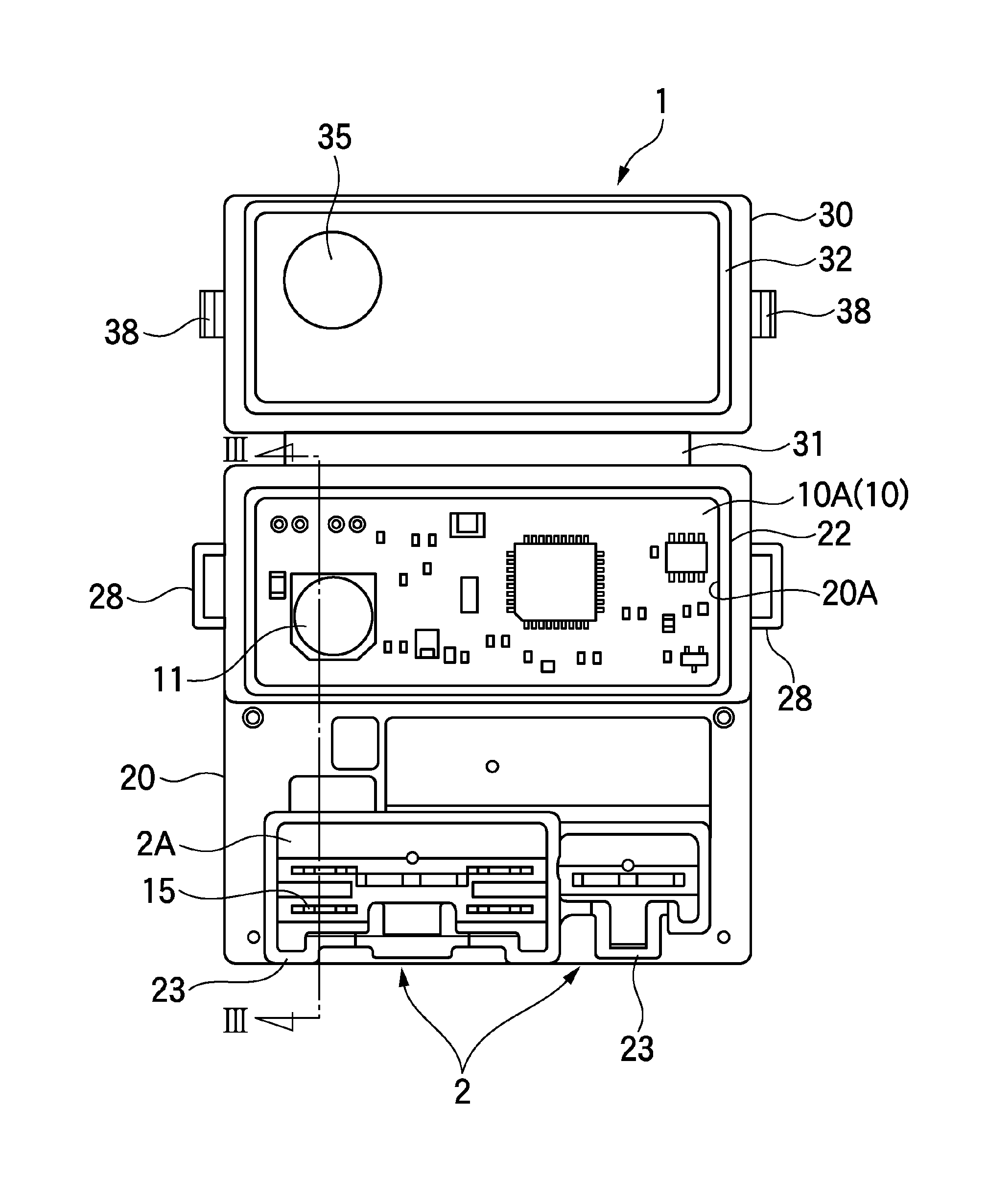
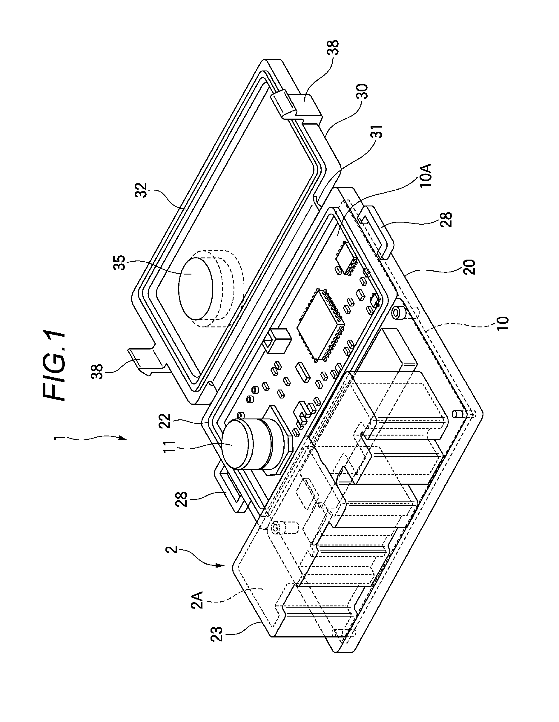
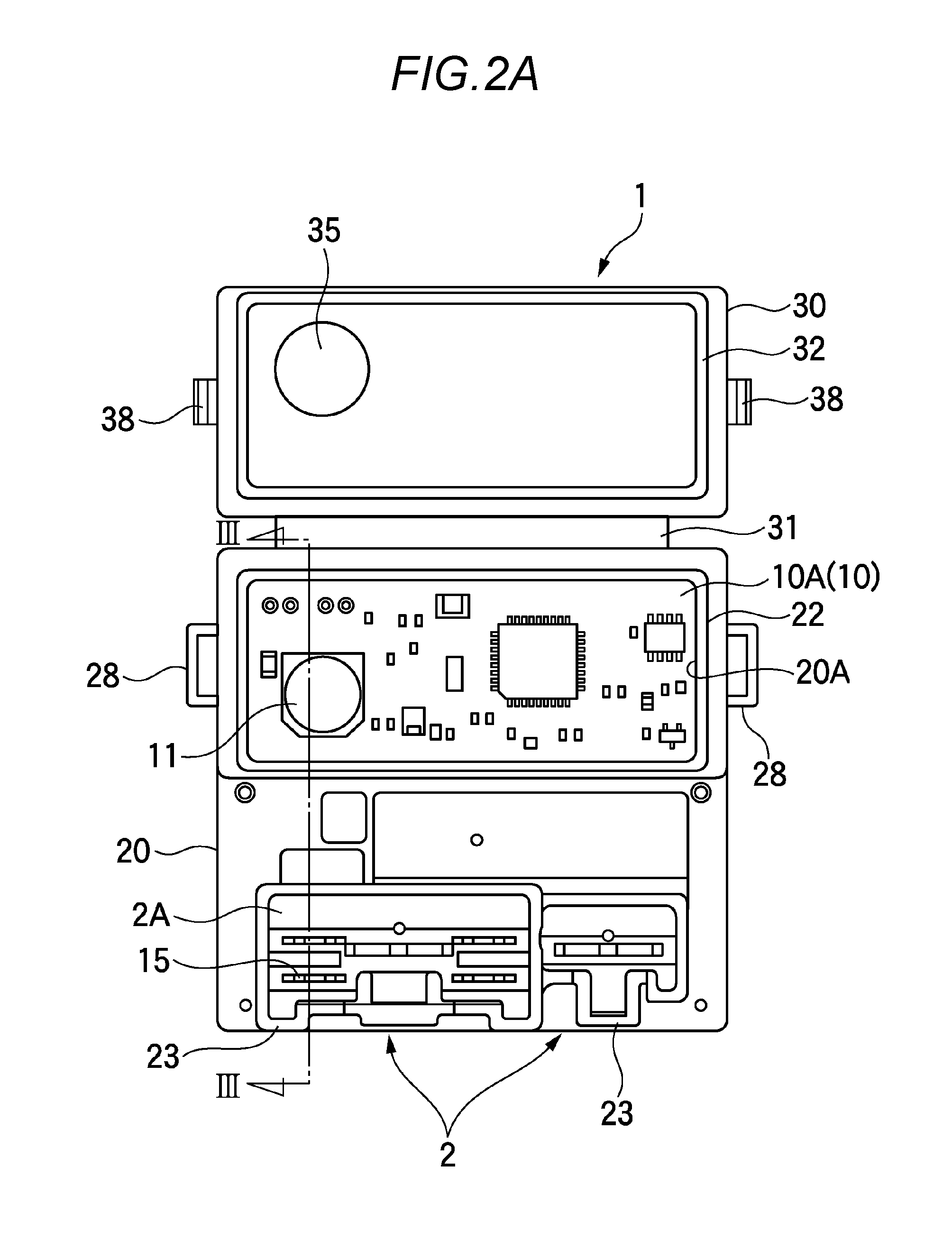
[0049]FIG. 1 is an external perspective view of an electronic circuit unit according to the FIGS. 2A to 2C are configuration diagrams of the electronic circuit unit, wherein FIGS. 2A, 2B and 2C are a top view, a side view and a bottom view of the unit, respectively. FIG. 3 is a sectional view taken along line in FIG. 2A.
[0050]As shown in FIGS. 1 to 2C, the electronic circuit unit 1 according to the first embodiment is configured in a manner that a mold exclusion part 10A is provided at a part of a plate surface of a rectangular circuit board 10 which mounts electronic components 11 thereon and is covered in its whole circumference by an outer case 20 formed by mold resin. In the mold exclusion part, a rear surface side is covered by the mold resin, and a front surface side is not covered by the mold resin but exposed from the outer case 20.
[0051]A connector housing 23 constituting a connector 2 is integrally formed with the outer case 20 of the electronic circuit unit 1. The connec...
second embodiment
[0071]Hereinafter, the second embodiment according to the invention will be explained with reference to drawings.
[0072]FIG. 4 is an external perspective view of an electronic circuit unit according to the second embodiment. FIGS. 5A to 5C are configuration diagrams of the electronic circuit unit, wherein FIGS. 5A, 5B and 5C are a top view, a side view and a bottom view of the unit, respectively. FIG. 6 is a sectional view taken along line VI-VI in FIG. 5A.
[0073]As shown in FIGS. 5 to 6C, the electronic circuit unit 1 according to the second embodiment is configured in a manner that a mold exclusion part 10A is provided at a part of a plate surface of a rectangular circuit board 10 which mounts electronic components 11 thereon and is covered in its whole circumference by an outer case 20 formed by mold resin. In the mold exclusion part, a rear surface side is covered by the mold resin, and a front surface side is not covered by the mold resin but exposed from the outer case 20.
[0074]...
third embodiment
[0090]Next, an electronic circuit unit according to the invention will be explained.
[0091]FIG. 7 is a sectional view of a portion, similar to that shown in FIG. 6, of the electronic circuit unit according to the third embodiment.
[0092]In the second embodiment described above, as the strength increasing part, the dummy reinforcement conductor pattern 12A is provided in the inner layer of the mold exclusion part 10A. In the electronic circuit unit according to the third embodiment, as shown in FIG. 7, a thickness increasing part 12B, formed by locally increasing a thickness of the conductor wring pattern 12, is provided at a part of the conductor wring pattern 12 on the inner layer of the circuit board 10 at the mold exclusion part 10A, as a strength increasing part.
[0093]The thickness increasing part 12B of the conductor wring pattern 12 is formed by locally increasing a thickness of the copper foil at a portion of the pattern where an elastic modulus is supposed to reduce. This thic...
PUM
 Abstract
Description
Claims
Application Information
 - R&D
- Intellectual Property
- Life Sciences
- Materials
- Tech Scout
- Unparalleled Data Quality
- Higher Quality Content
- 60% Fewer Hallucinations
Browse by: Latest US Patents, China's latest patents, Technical Efficacy Thesaurus, Application Domain, Technology Topic, Popular Technical Reports.
© 2025 PatSnap. All rights reserved.Legal|Privacy policy|Modern Slavery Act Transparency Statement|Sitemap|About US| Contact US: help@patsnap.com


