Electronic component module and manufacturing method thereof

a technology of electronic components and manufacturing methods, applied in the direction of cross-talk/noise/interference reduction, printed circuit non-printed electric components association, semiconductor/solid-state device details, etc., can solve the problems of low electromagnetic wave shielding effect and manufacturing efficiency reduction, and achieve the effect of low manufacturing efficiency

Active Publication Date: 2016-09-22
SAE MAGNETICS (HK) LTD
View PDF7 Cites 1 Cited by
  • Summary
  • Abstract
  • Description
  • Claims
  • Application Information

AI Technical Summary

Benefits of technology

This patent aims to provide an electronic component module and a manufacturing method that can solve problems of low electromagnetic wave shielding and low manufacturing efficiency. The module has a metal film covering the exterior surface of the insulating body, the side surface of the substrate, and the top surface of the recess portion formed in the substrate. This improves the electromagnetic wave shielding effect. The manufacturing process prevents the metal film from being formed in the recess portion, which makes it easier to detach the sheet member. This increases the manufacturing efficiency.

Problems solved by technology

This causes a problem of low electromagnetic wave shielding effect with respect to an electromagnetic component module.
As such, a plurality of numbers of electronic component modules cannot be manufactured at once, causing a problem that the manufacturing efficiency is lowered.

Method used


Image

  • Electronic component module and manufacturing method thereof
  • Electronic component module and manufacturing method thereof
  • Electronic component module and manufacturing method thereof

Examples


Embodiment Construction

[0030]Various preferred embodiments of the invention will now be described with reference to the figures, wherein like reference numerals designate similar parts throughout the various views. As indicated above, the invention is directed to an electronic component module which can improve electromagnetic wave shielding effect.

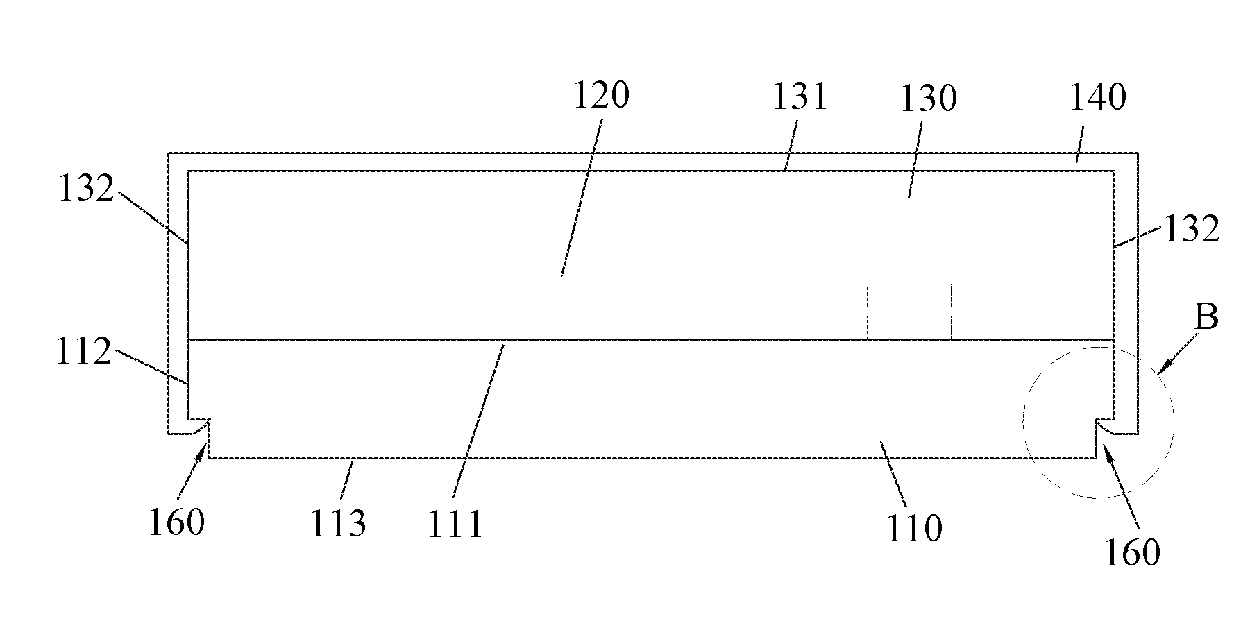
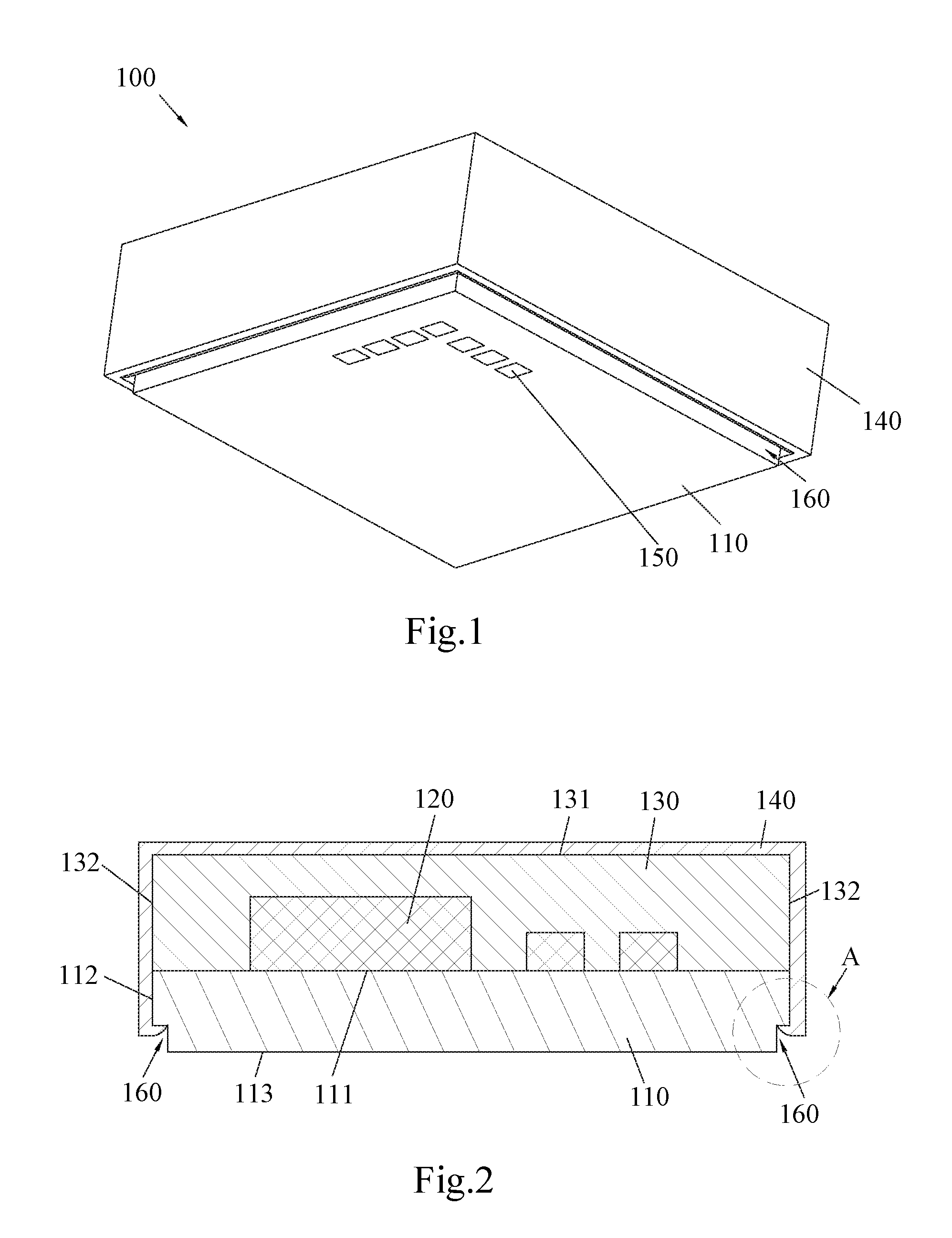
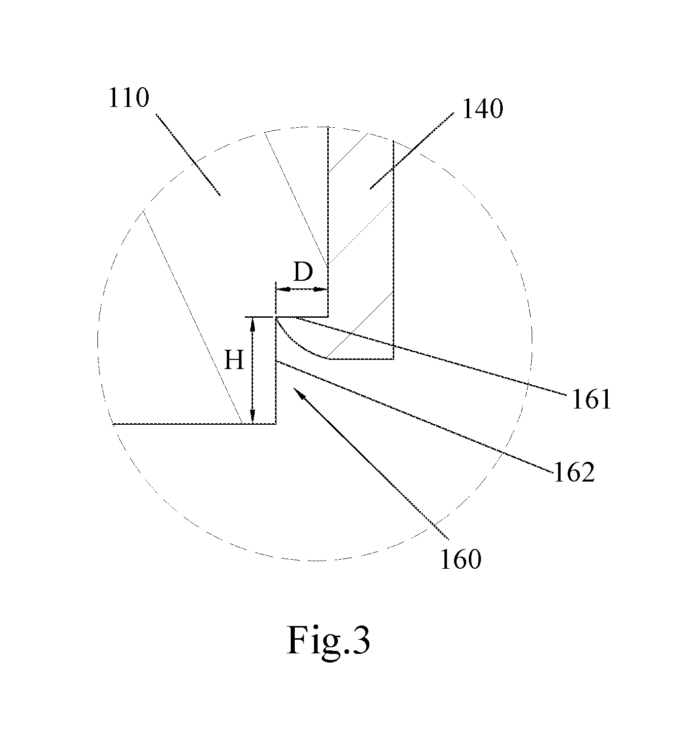
[0031]FIGS. 1˜3 show an electronic component module according to a first embodiment of the present invention. FIG. 1 shows a perspective view of an electronic component module according to the present invention. FIG. 2 is a cross-sectional view of the electronic component module 100 of FIG. 1. FIG. 3 is a partial enlarged view of the portion A in FIG. 2. As illustrated, the electronic component module 100 includes a substrate 110 having an electronic component mounting surface 111 for mounting electronic components 120 and a connection terminal formation surface 113 for forming connection terminals 150 opposite each other, electronic components 120 mounted on t...


PUM


Abstract

An electronic component module includes a substrate; at least one electronic component mounted on an electronic component mounting surface of the substrate; an insulating body covering the electronic component on the electronic component mounting surface of the substrate; and a metal film formed by sputtering, the metal film covering at least one exterior surface of the insulating body and at least one side surface of the substrate. The substrate has a recess portion formed on a periphery of the surface of the substrate that is opposite to the electronic component mounting surface, and the recess portion has a top surface parallel to the electronic component mounting surface and a side surface perpendicular to the top surface, and the metal film is extended to cover the top surface of the recess portion, without covering the side surface thereof. It obtains improved electromagnetic wave shielding effect and improved manufacturing efficiency.

Description

RELATED APPLICATIONS[0001]This application claims the benefit of priority to Chinese Patent Application No. 201520154542.4 filed in Mar. 18, 2015, which is hereby incorporated by reference in its entirety.FIELD OF THE INVENTION[0002]The present invention relates to electronic component modules, and in particular, to electronic component modules having electromagnetic wave shields.BACKGROUND OF THE INVENTION[0003]In order to take measures against electromagnetic waves such as prevention of electromagnetic wave leakage or electromagnetic wave penetration with respect to electronic components, electronic components are covered with electromagnetic wave shields in their peripheries. For example, JP 2003-142626 A (Patent Document 1) discloses a technique of covering the periphery of a semiconductor chip mounted on a substrate with a metal cap provided on the substrate. JP 2006-332255 A (Patent Document 2) discloses a technique of covering the periphery of a semiconductor chip mounted on ...

Claims


Application Information

Patent Timeline
Patent Type & Authority Applications(United States)
IPC IPC(8): H05K1/02H05K3/30H05K1/18
CPCH05K1/0216H05K3/30H05K1/183H05K1/0218H05K3/0097H05K2201/0317H05K2201/0715H05K2201/09145H05K2201/09845H01L21/561H01L21/568H01L23/552H01L24/97H01L2924/15159H01L2924/15313H05K3/284
Inventor NAKAO, AKIO
Owner SAE MAGNETICS (HK) LTD
Why Eureka
Try Eureka