Dual-gate TFT array substrate and manufacturing method thereof

a technology of thin film transistors and array substrates, applied in the field of display, can solve the problems of increasing process complexity and manufacturing costs, improving manufacturing efficiency, etc., and achieve the effect of reducing manufacturing efficiency and complex manufacturing process

Active Publication Date: 2017-12-28
TCL CHINA STAR OPTOELECTRONICS TECH CO LTD
View PDF5 Cites 2 Cited by
  • Summary
  • Abstract
  • Description
  • Claims
  • Application Information

AI Technical Summary

Benefits of technology

[0005]The object of the present invention is to provide an improved dual-gate TFT (thin film transistor) array substrate and a manufacturing method thereof to solve the problems existing in a traditional dual-gate TFT array substrate: a complex manufacturing process and lower manufacturing efficiency.

Problems solved by technology

Thus, an increased number of masks is required, so that the process complexity and the manufacturing cost are increased, which is disadvantageous to improving the manufacturing efficiency.

Method used


Image

  • Dual-gate TFT array substrate and manufacturing method thereof
  • Dual-gate TFT array substrate and manufacturing method thereof
  • Dual-gate TFT array substrate and manufacturing method thereof

Examples


Embodiment Construction

[0022]The foregoing objects, features, and advantages adopted by the present invention can be best understood by referring to the following detailed description of the preferred embodiments and the accompanying drawings. Furthermore, the directional terms described in the present invention, such as upper, lower, front, rear, left, right, inside, outer, side, etc., are only directions with reference to the accompanying drawings, so that the used directional terms are used to describe and understand the present invention, but the present invention is not limited thereto.

[0023]In the drawings, units with similar structures use the same numerals.

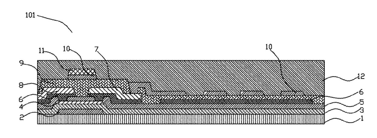
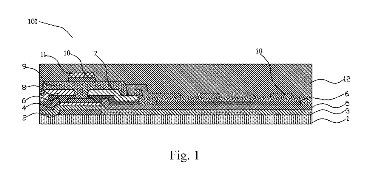
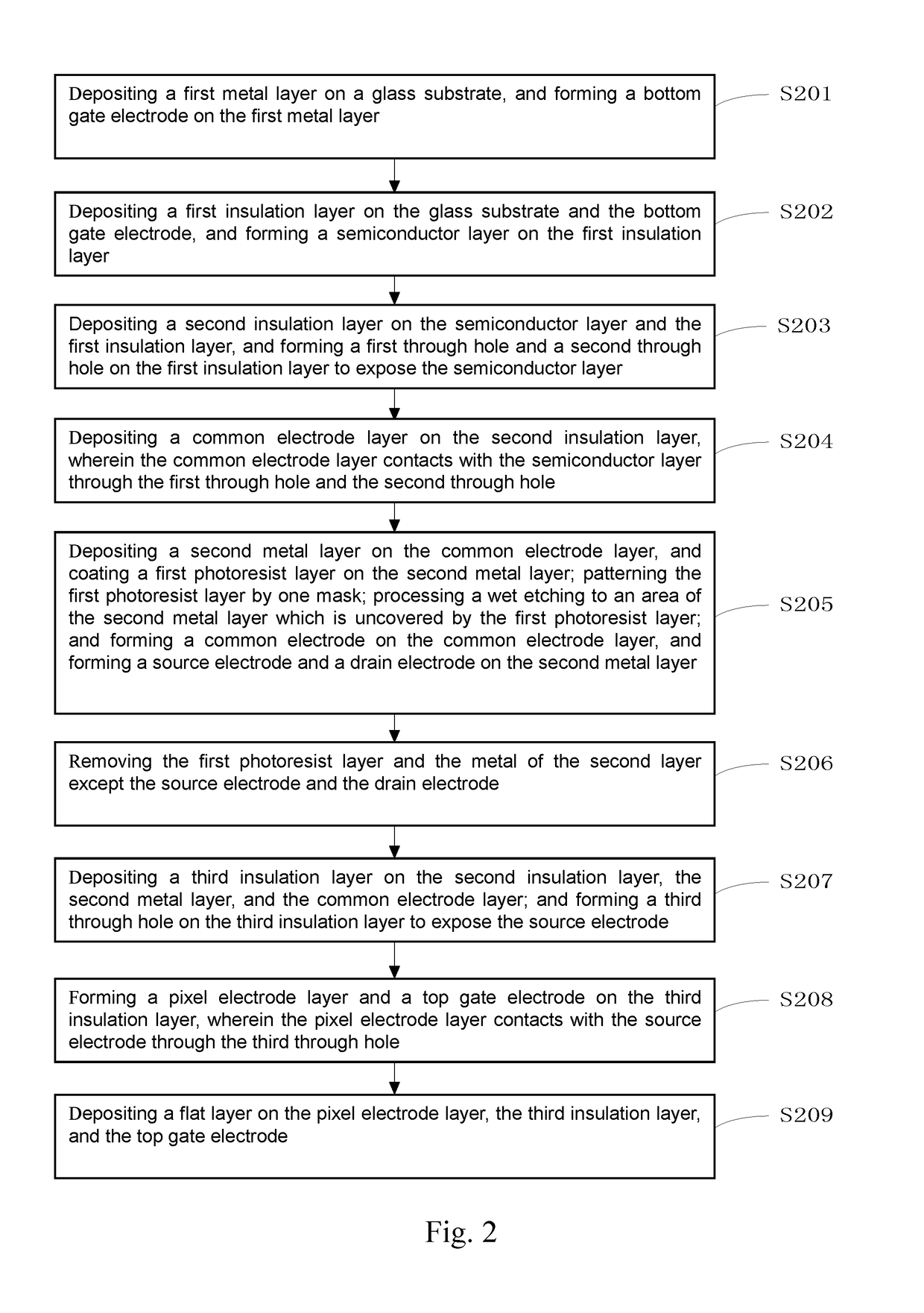
[0024]Refer now to FIG. 1, which is a schematic structural view of a dual-gate TFT array substrate according to a preferred embodiment of the present invention. A dual-gate TFT array substrate 101 according to the preferred embodiment comprises: a glass substrate 1, a bottom gate electrode 2, a first insulation layer 3, a semiconductor layer 4, ...


PUM

PropertyMeasurementUnit
areaaaaaaaaaaa
semiconductoraaaaaaaaaa
stabilityaaaaaaaaaa

Abstract

A dual-gate TFT (thin film transistor) array substrate and a manufacturing method thereof are provided. A source electrode and a drain electrode are formed on a common electrode layer; and a common electrode of the common electrode layer, the source electrode and the drain electrode can simultaneously be formed by one mask during manufacturing. Therefore, the dual-gate TFT array substrate and the manufacturing method thereof have beneficial effects to reduce the number of masks, shorten the process, and improve the manufacturing efficiency.

Description

FIELD OF THE INVENTION[0001]The present invention relates to a display field, and more particularly to a dual-gate TFT (thin film transistor) array substrate and a manufacturing method thereof.BACKGROUND OF THE INVENTION[0002]In traditional liquid crystal display technologies, for improving the stability of an oxide TFT (thin film transistor) in a dual-gate TFT array substrate, an etch stop layer (ESL) structure is widely adopted, and the structure can efficaciously decrease influences for back channels from external environment factors and etching damages of source and drain electrodes.[0003]In an active array display device, a single-gate TFT is commonly adopted. But the dual-gate TFT has the advantages of: higher mobility, greater on-state current, smaller threshold swing, better threshold voltage stability, better uniformity, and has better gate bias stability.[0004]However, in a manufacturing method of a dual-gate TFT array substrate of a traditional FFS (fringe field switching...

Claims


Application Information

Patent Timeline
Patent Type & Authority Applications(United States)
IPC IPC(8): H01L29/49H01L29/78H01L29/66H01L29/417H01L29/06H01L29/786G02F1/1343
CPCH01L29/4908H01L29/66969H01L29/785H01L29/41733H01L29/78618G02F1/1343H01L29/0653H01L27/124H01L27/1288G02F1/1368H01L29/78648H01L29/7869H01L27/1225
Inventor GE, SHIMIN
Owner TCL CHINA STAR OPTOELECTRONICS TECH CO LTD
Why Eureka
Try Eureka