Superconducting wire material having laminated structure and manufacturing method therefor
- Summary
- Abstract
- Description
- Claims
- Application Information
AI Technical Summary
Benefits of technology
Problems solved by technology
Method used
Image

Examples
Embodiment Construction
[0029]Hereinafter, the present invention will be described by explaining preferable embodiments of the present invention with reference to the drawings.
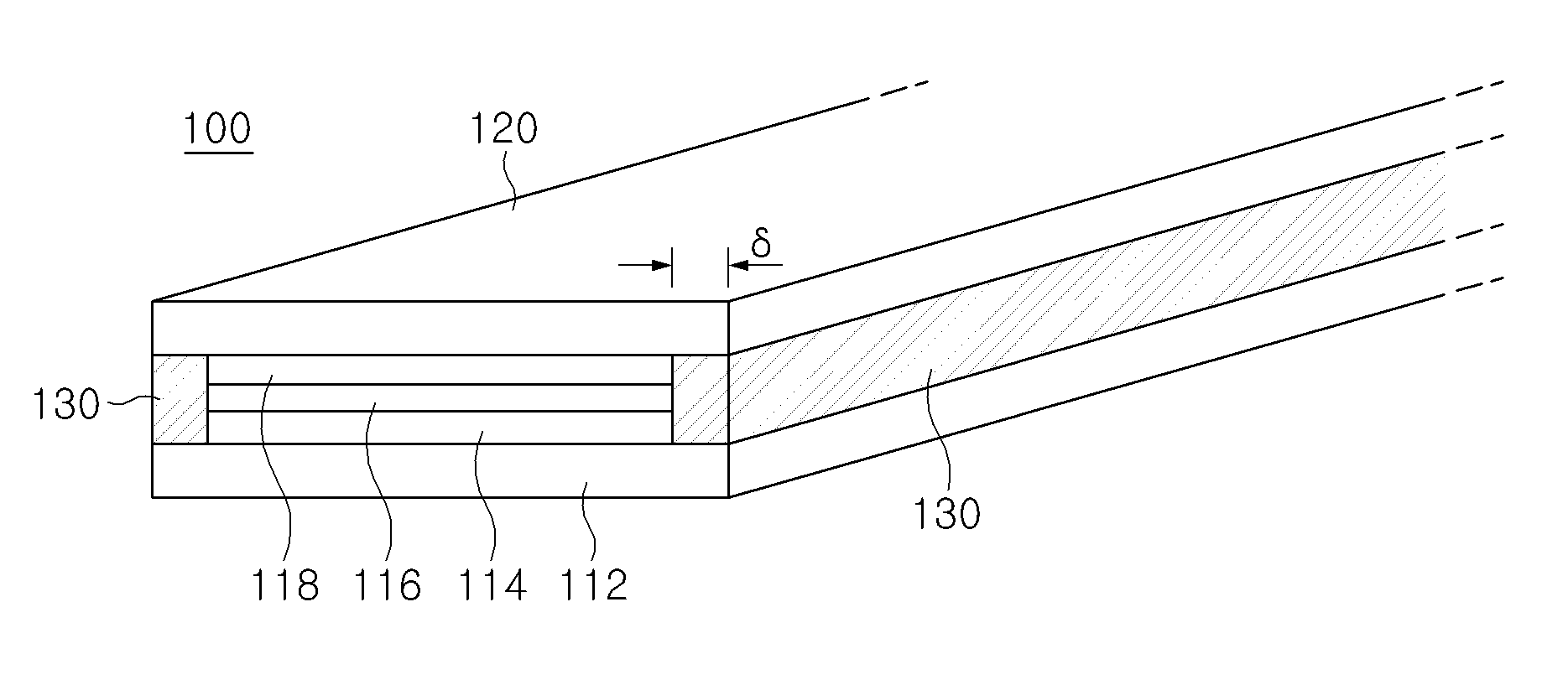
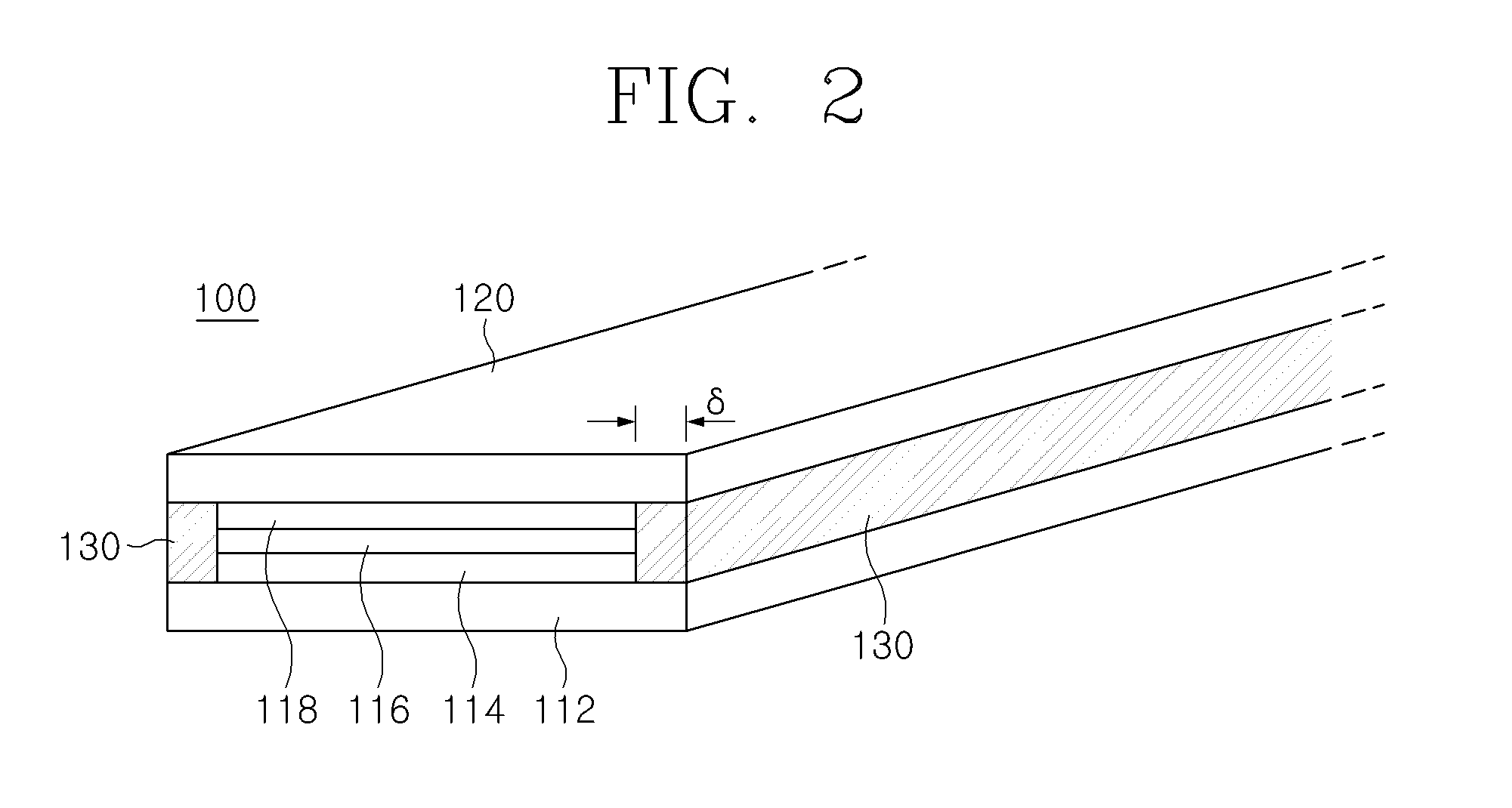
[0030]FIG. 2 is an exemplary view illustrating a superconducting wire material having a laminated structure according to a preferable embodiment of the present invention.
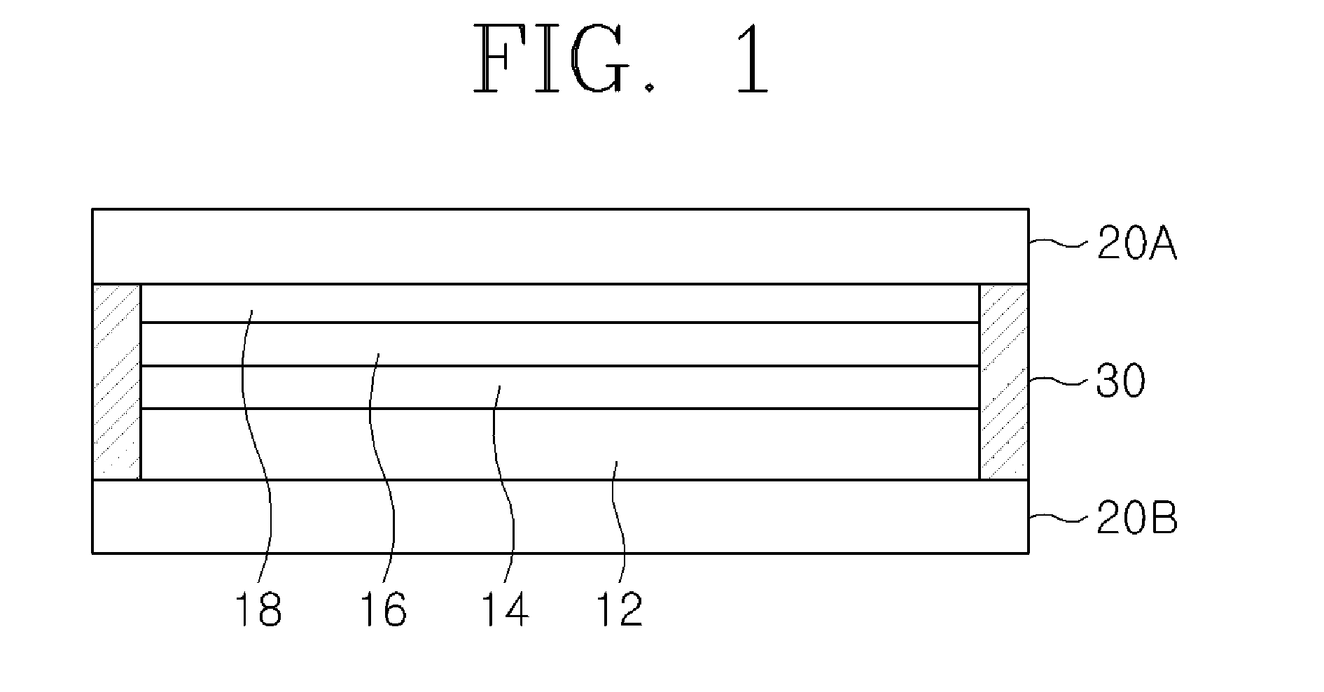
[0031]Referring to FIG. 2, a superconducting wire material 100 has a strip shape of a predetermined width extending in a longitudinal direction. The superconducting wire material includes a laminated structure of a deposition substrate 112, a buffer layer 114, a superconducting layer 116, a stabilization layer and a lamination substrate 120.
[0032]A structure of the deposition substrate 112, the buffer layer 114, the superconducting layer 116 and the stabilization layer 118 forming the wire material 110 of the present invention and a method for manufacturing the same may be manufactured by a typical method which is obvious to a skilled person in the art to which the p...
PUM
| Property | Measurement | Unit |
|---|---|---|
| Width | aaaaa | aaaaa |
| Superconductivity | aaaaa | aaaaa |
Abstract
Description
Claims
Application Information
 - R&D
- Intellectual Property
- Life Sciences
- Materials
- Tech Scout
- Unparalleled Data Quality
- Higher Quality Content
- 60% Fewer Hallucinations
Browse by: Latest US Patents, China's latest patents, Technical Efficacy Thesaurus, Application Domain, Technology Topic, Popular Technical Reports.
© 2025 PatSnap. All rights reserved.Legal|Privacy policy|Modern Slavery Act Transparency Statement|Sitemap|About US| Contact US: help@patsnap.com