
Substrate structure and fabrication method thereof

a technology of substrate structure and fabrication method, which is applied in the direction of lithographic mask, conductive pattern formation, printed element electric connection formation, etc., can solve the problems of warping of the overall package structure and easy so as to reduce the variation in the size of the dielectric layer, strengthen the substrate structure, and reduce the effect of thermal warping of the substrate structur

Active Publication Date: 2016-05-05
SILICONWARE PRECISION IND CO LTD
View PDF14 Cites 1 Cited by
  • Summary
  • Abstract
  • Description
  • Claims
  • Application Information

AI Technical Summary

Benefits of technology

The patent text describes a method of strengthening the structure of a substrate and reducing the variation in the size of the dielectric layer. This reduces the thermal warping of the substrate and improves its stability.

Problems solved by technology

However, when the substrate structure is bonded with a chip and subjected to a molding process for forming a package structure, thermal warping easily occurs to the substrate structure.
On the other hand, the molding compound generally has a thickness too small (for example, less than 0.5 mm) to overcome or balance thermal warping stresses, thus leading to warping of the overall package structure.

Method used


Image

  • Substrate structure and fabrication method thereof
  • Substrate structure and fabrication method thereof
  • Substrate structure and fabrication method thereof

Examples


Embodiment Construction

[0024]The following illustrative embodiments are provided to illustrate the disclosure of the present invention, these and other advantages and effects can be apparent to those in the art after reading this specification.

[0025]It should be noted that all the drawings are not intended to limit the present invention. Various modifications and variations can be made without departing from the spirit of the present invention. Further, terms such as “first”, “second”, “on”, “a” etc. are merely for illustrative purposes and should not be construed to limit the scope of the present invention.

[0026]FIGS. 2A to 2H are schematic cross-sectional views showing a method for fabricating a substrate structure according to the present invention.

[0027]Referring to FIG. 2A, a carrier 20 having opposite first and second surfaces is provided and at least a strengthening member 27 is disposed on the first and second surfaces of the carrier 20. The strengthening member 27 can be made of a laminating comp...


PUM

PropertyMeasurementUnit
thicknessaaaaaaaaaa
strengthaaaaaaaaaa
dielectricaaaaaaaaaa

Abstract

A method for fabricating a substrate structure is provided, which includes the steps of: disposing at least a strengthening member on a carrier; sequentially forming a first circuit layer and a dielectric layer on the carrier, wherein the strengthening member is embedded in the dielectric layer; forming a second circuit layer on the dielectric layer; removing the carrier; and forming an insulating layer on the first circuit layer and the second circuit layer. The strengthening member facilitates to reduce thermal warping of the substrate structure.

Description

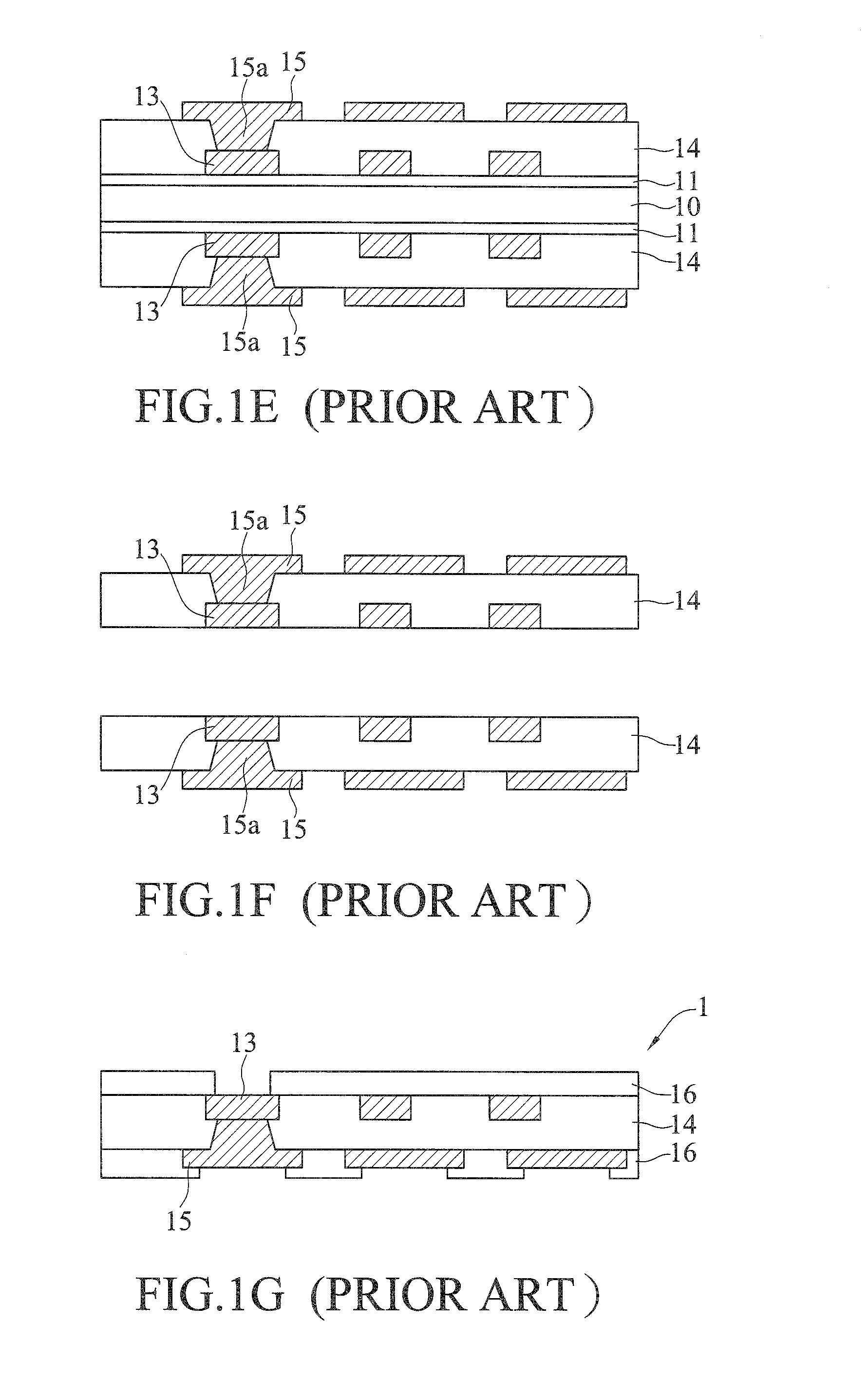
BACKGROUND OF THE INVENTION[0001]1. Field of the Invention[0002]The present invention relates to substrate structures and fabrication methods thereof, and more particularly, to a substrate structure and a fabrication method thereof for reducing thermal warping.[0003]2. Description of Related Art[0004]Along with the rapid development of electronic industries, electronic products are required to be reduced in thickness, and accordingly thin type substrates are needed.[0005]FIGS. 1A to 1G are schematic cross-sectional views showing a method for fabricating a substrate structure according to the prior art.[0006]Referring to FIG. 1A, a carrier 10 is provided and a seed layer 11 is formed on opposite surfaces of the carrier 10.[0007]Referring to FIG. 1B, a patterned resist layer 12 having a plurality of openings is formed on the seed layer 11. Thereafter, a first circuit layer 13 is formed in the openings of the patterned resist layer 12 by electroplating.[0008]Referring to FIG. 1C, the p...

Claims


Application Information

Patent Timeline
Patent Type & Authority Applications(United States)
IPC IPC(8): H05K1/02H05K3/40H05K1/11H05K3/00H05K3/06
CPCH05K1/0298H05K3/007H05K3/0011H05K2203/0548H05K1/115H05K3/4038H05K1/0271H05K3/06H05K3/184H05K3/4682H05K2201/0187H05K2201/096H05K2203/0709H05K2203/0147H05K2203/0156H05K2203/0165Y10T29/49155
Inventor YOU, JIN-WEICHEN, CHUN-LUNG
Owner SILICONWARE PRECISION IND CO LTD
Learn More