In-Cell Touch Liquid Crystal Display Apparatus, Method Of Manufacturing The Same, Method Of Manufacturing Thin Film Transistor Array Substrate, And Method Of Manufacturing Color Filter Array Substrate

a liquid crystal display and cell technology, applied in the field of cell touch liquid crystal display apparatus, can solve the problems of inability to develop many limitations of difficulty in applying in-cell touch lcd devices based on the tn mod

Active Publication Date: 2016-05-05
LG DISPLAY CO LTD
View PDF4 Cites 31 Cited by
  • Summary
  • Abstract
  • Description
  • Claims
  • Application Information

AI Technical Summary

Benefits of technology

[0018]Accordingly, the disclosed embodiments describe an in-cell touch liquid crystal display (LCD) device based on a twisted nematic (TN) mode, a method of manufacturing the same, a method of manufacturing a

Problems solved by technology

However, there are many limitations in applying the in-cell touch type to LCD devices based on the TN mode.
Since the related art LCD device based on the TN mode has a structure where a common electrode is spread all over a color filter array s

Method used


Image

  • In-Cell Touch Liquid Crystal Display Apparatus, Method Of Manufacturing The Same, Method Of Manufacturing Thin Film Transistor Array Substrate, And Method Of Manufacturing Color Filter Array Substrate
  • In-Cell Touch Liquid Crystal Display Apparatus, Method Of Manufacturing The Same, Method Of Manufacturing Thin Film Transistor Array Substrate, And Method Of Manufacturing Color Filter Array Substrate
  • In-Cell Touch Liquid Crystal Display Apparatus, Method Of Manufacturing The Same, Method Of Manufacturing Thin Film Transistor Array Substrate, And Method Of Manufacturing Color Filter Array Substrate

Examples


Embodiment Construction

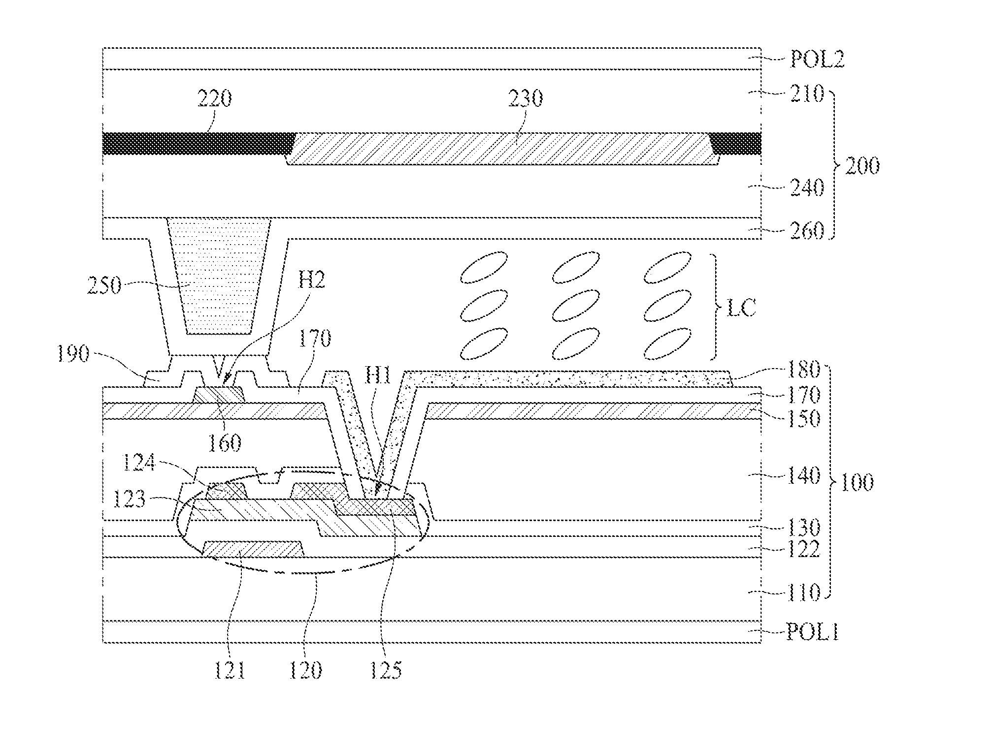
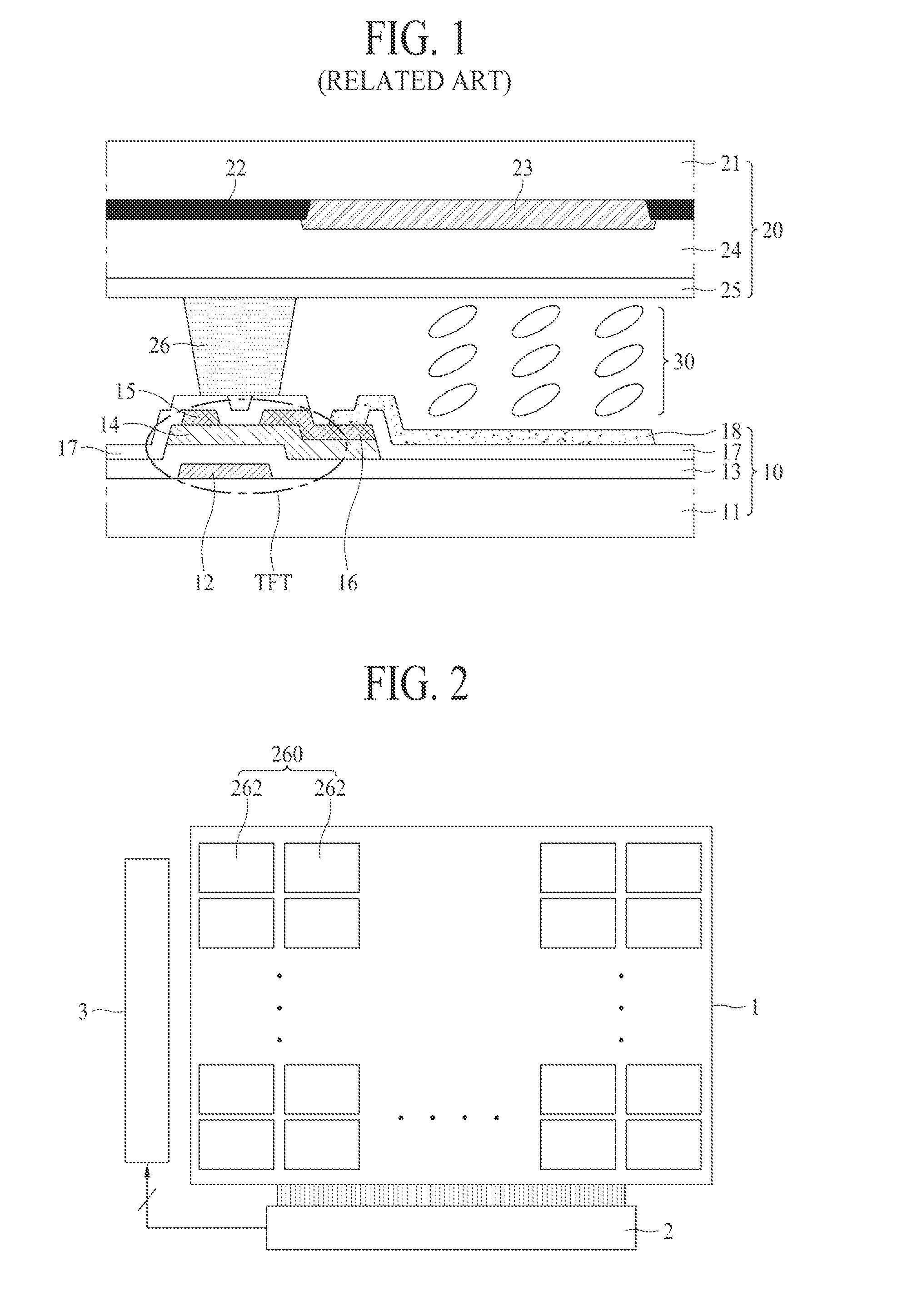
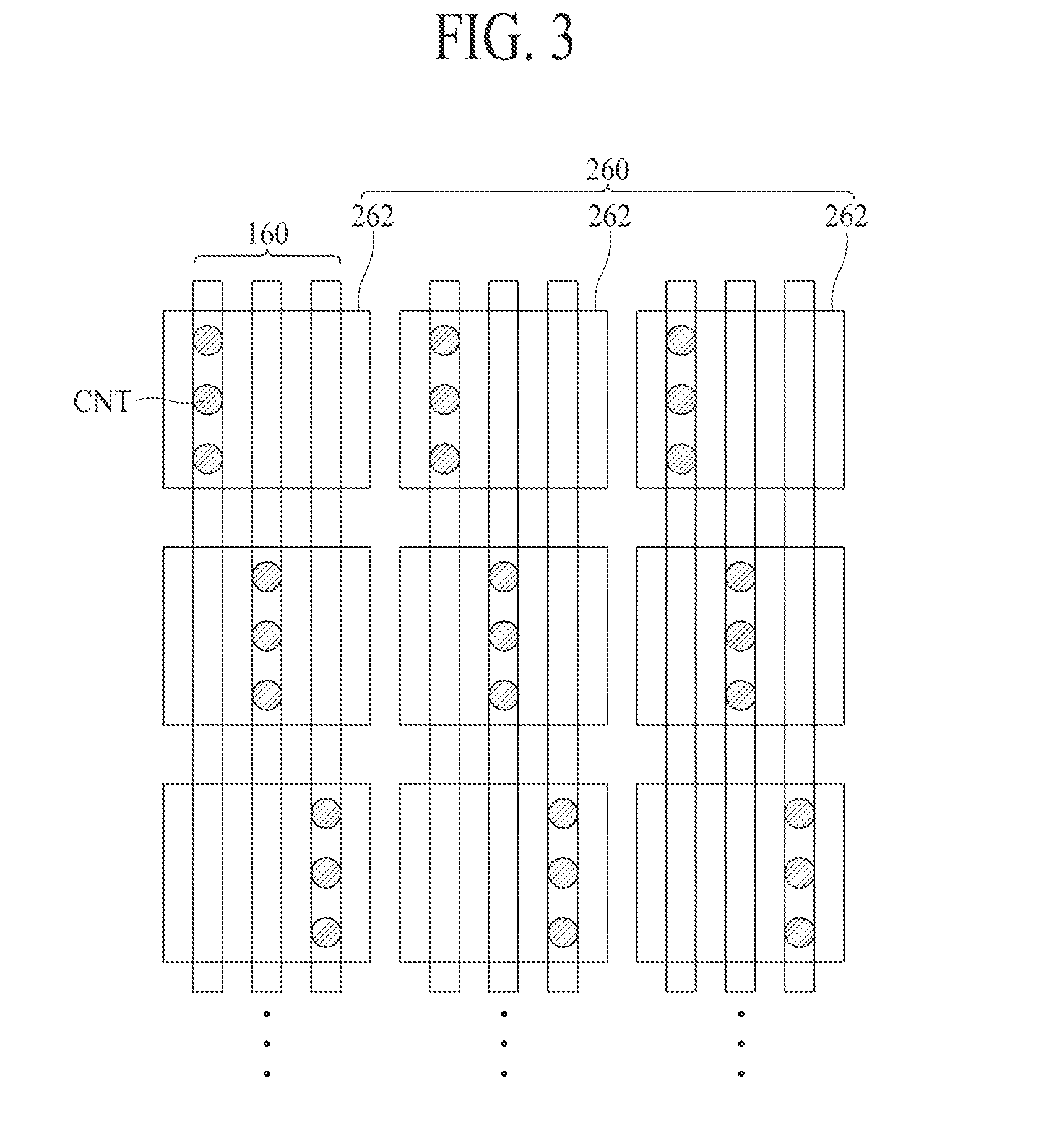
[0039]Reference will now be made in detail to the example embodiments that are illustrated in the accompanying drawings. Wherever possible, the same reference numbers will be used throughout the drawings to refer to the same or like parts.

[0040]Advantages and features of the present invention, and implementation methods thereof will be clarified through the following embodiments described with reference to the accompanying drawings. The present invention may, however, be embodied in different forms and should not be construed as being limited to the embodiments set forth herein. Rather, these embodiments are provided so that this disclosure will be thorough, and will fully convey the scope of the present invention to those skilled in the art. Furthermore, the present invention is defined by the scope of the claims.

[0041]Any shape, size, ratio, angle, or number disclosed in the drawings for describing an embodiment is merely an example, and thus, the present invention is not limited ...


PUM


Abstract

Disclosed are an in-cell touch liquid crystal display (LCD) device based on a twisted nematic (TN) mode, a method of manufacturing the same, a method of manufacturing a thin film transistor (TFT) array substrate, and a method of manufacturing a color filter array substrate. The TFT array substrate includes a TFT disposed in a pixel area defined by an intersecting gate line and data line, a conductive line disposed on the TFT, and a transparent conductive layer in electrical contact with the conductive line. The color filter array substrate includes a light shield layer, a color filter, an overcoat layer covering the light shield layer and the color filter, a column spacer disposed on the overcoat layer, and a common electrode disposed on the overcoat layer and the column spacer, where the conductive line supplies the common electrode with a common voltage or a touch driving signal.

Description

CROSS-REFERENCE TO RELATED APPLICATIONS[0001]This application claims the benefit of the Korean Patent Application No. 10-2014-0150667 filed on Oct. 31, 2014, which is hereby incorporated by reference as if fully set forth herein.BACKGROUND[0002]1. Field of the Invention[0003]The disclosed embodiments relate to an in-cell touch liquid crystal display (LCD) device based on a twisted nematic (TN) mode, a method of manufacturing the same, a method of manufacturing a thin film transistor (TFT) array substrate, and a method of manufacturing a color filter array substrate.[0004]2. Discussion of the Related Art[0005]As portable electronic devices (e.g., mobile phones, tablet personal computers (PCs), notebook computers) and display devices (e.g., monitors, televisions (TVs)) advance, the demand for applicable flat panel display (FPD) devices is increasing.[0006]FPD devices include liquid crystal display (LCD) devices, plasma display panels (PDPs), field emission display (FED) devices, and o...

Claims


Application Information

Patent Timeline
IPC IPC(8): G02F1/1362G02F1/1333G02F1/1339G02F1/1335G02F1/1368
CPCG02F1/136286G02F1/133514G02F1/1368G02F2001/136295G02F1/13394G02F1/13338G02F2001/133519G02F1/133512
Inventor PARK, YONG CHANKIM, JIN SEONGKIM, SEUNG KYEOM
Owner LG DISPLAY CO LTD
Why Eureka
Try Eureka