
Carrier wafer, method for holding a flexible substrate and method for the manufacture of a carrier wafer

a carrier wafer and flexible technology, applied in the direction of solid-state device manufacturing, electric devices, solid-state devices, etc., can solve the problems of bending under the weight and inertia of the substrate, affecting the production efficiency of the substrate, so as to avoid unnecessary repetition and improve the effect of invention

Active Publication Date: 2016-02-04
FRAUNHOFER GESELLSCHAFT ZUR FOERDERUNG DER ANGEWANDTEN FORSCHUNG EV
View PDF4 Cites 6 Cited by
  • Summary
  • Abstract
  • Description
  • Claims
  • Application Information

AI Technical Summary

Benefits of technology

The invention relates to a method for producing a carrier wafer, which can securely hold and charge multiple electrodes that may have defects in their insulation. The method involves using a common feeder conductor for all the floating electrodes and irradiating them with UV light to discharge them. This allows for the easy removal of a flexible thin substrate from the carrier wafer. The technical effects of this invention include securing long-term charging of multiple electrodes, ease of construction, and improved efficiency in the production process.

Problems solved by technology

One problem in the handling of such thin substrates is the danger that the substrate may break.
Thin substrates of this type also lose their stability and bend under their own weight and inertia, frequently by several millimeters.
Therefore normal handling devices that remove the substrate from a kiln and transport it through various processing stations can no longer be used.
An additional problem is presented by the sharp edges of the thin substrates, which cause problems during transport and handling.
In certain situations the use of adhesives or films is not appropriate, e.g. because they would be destroyed by high temperatures or by certain chemicals.
Under some conditions, adhesive residue remains on the surface of the substrate after the substrate has been processed and removed from the carrier wafer, which results in the undesirable contamination of the equipment.
However, the electrostatic chuck described above is a stationary component of the plasma plant and therefore cannot be transported together with the substrate between different processing stations.
Even extremely small leaks in the insulation would result directly in the discharge of the floating electrode, so that it would no longer be suitable for the long-term holding of a thin utilizable wafer.
A disadvantage with the carrier wafer known from DE 10 2006 555 618 A1 is that if there is the slightest defect in the insulation layers that insulate the electrode on all sides, a leakage current occurs that results in a discharge of the floating electrode.
Because the floating electrode in this carrier wafer has a large surface area, the probability of a defect in the insulation layer is very high, so that these carrier wafers frequently fail.

Method used


Image

  • Carrier wafer, method for holding a flexible substrate and method for the manufacture of a carrier wafer
  • Carrier wafer, method for holding a flexible substrate and method for the manufacture of a carrier wafer
  • Carrier wafer, method for holding a flexible substrate and method for the manufacture of a carrier wafer

Examples


Embodiment Construction

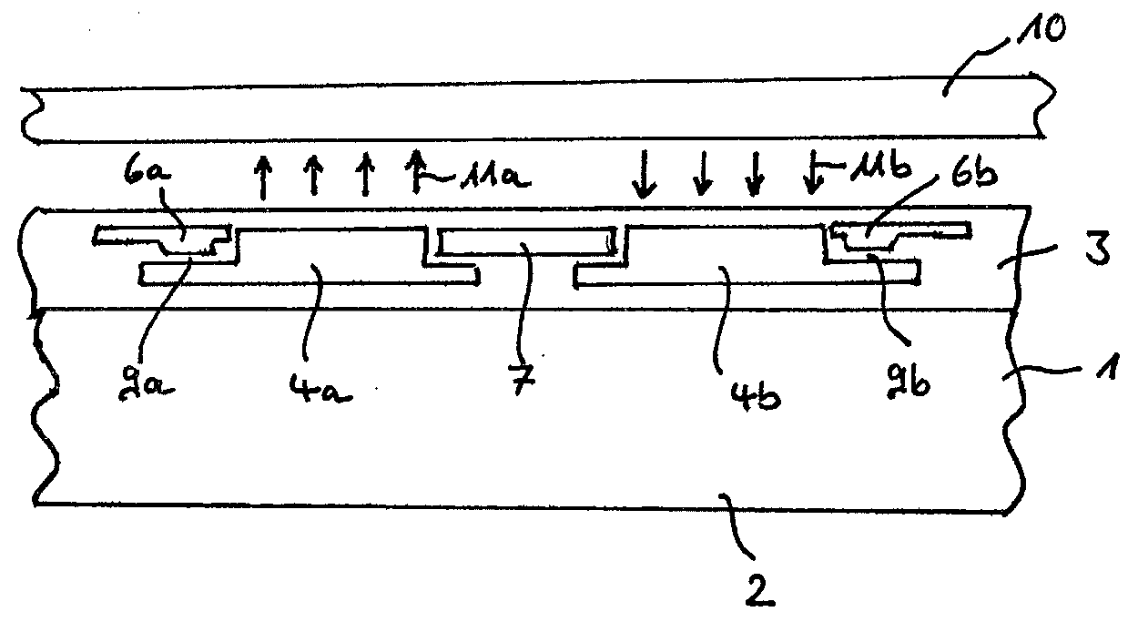
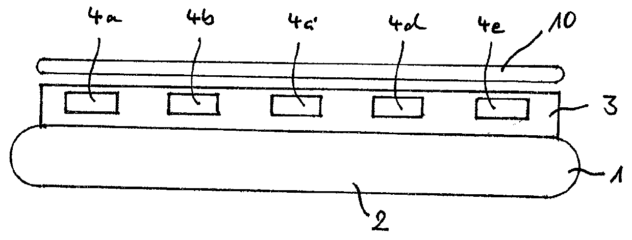
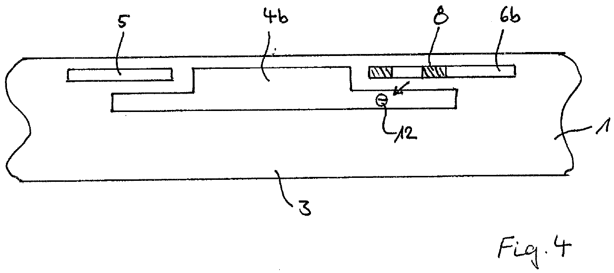
[0050]FIG. 1 shows a cross-section through a carrier wafer 1. This carrier wafer 1 has a substrate 2 on which an insulating layer 3 is located and embedded in the insulating layer 3 are electrodes 4a to 4e which are electrically insulated on all sides by the insulating layer 3. Electrodes of this type insulated on all sides are also called floating electrodes. They have no defined potential.

[0051]According to the invention, to hold a utilizable wafer 10, the floating electrodes 4a to 4e are charged with electrical charge carriers. For a unipolar carrier wafer 1 this charge can be delivered by means of identical charge carriers, e.g. only with electrons. For a bipolar carrier wafer, the floating electrodes located next to one another can be charged with charge carriers of different polarity, e.g. the floating electrodes 4a, 4c and 4e can be charged with electrons and the floating electrodes 4b and 4d can be charged with holes.

[0052]The floating electrodes 4a to 4e charged in this man...


PUM


Abstract

Carrier wafers are used to hold thin and ultra-thin substrates such as semiconductor components, for example. The carrier wafer of the invention has a plurality of electrodes insulated on all sides (floating electrodes). This plurality of floating electrodes, but at least 50 floating electrodes, are located next to one another with reference to the plane of the first surface of the carrier wafer. Each of these floating electrodes can be charged, for example by means of Fowler-Nordheim tunnels or by the injection of hot charge carriers, in particular of hot electrons or hot holes. Also provided are a method for holding a flexible substrate by means of a carrier wafer of this type and a method for the manufacture of a carrier wafer of this type.

Description

BACKGROUND OF THE INVENTION[0001]This invention relates to a carrier wafer, a method for holding a flexible substrate by means of a carrier wafer of this type and a method for the manufacture of a carrier wafer of this type. Carrier wafers are used to hold thin and ultra-thin substrates such as semiconductor components, for example.[0002]Thin semiconductor components have been widely used in the microelectronics industry in recent years. Examples of such uses are integrated circuits for chip cards in which the thickness of the silicon components is currently approximately 150 μm and less. Increasingly thinner wafers are also being used in the manufacture of solar cells. Chips with a thickness of 100 μm and less are also used in power semiconductors. Last but not least, electronic components made of organic semiconductors on thin plastic films are also used in polymer electronics, such as organic light-emitting diodes (OLED), for example.[0003]One problem in the handling of such thin...

Claims


Application Information

Patent Timeline
IPC IPC(8): H01L21/683H02N13/00
CPCH01L21/6833H01L2221/68381H01L21/6835H02N13/00
Inventor KUTTER, CHRISTOPHLANDESBERGER, CHRISTOFBOLLMANN, DIETER
Owner FRAUNHOFER GESELLSCHAFT ZUR FOERDERUNG DER ANGEWANDTEN FORSCHUNG EV
Learn More