Structure, wiring board and electronic device
a technology of wiring board and electronic device, applied in the direction of cross-talk/noise/interference reduction, printed circuit details, electrical connection printed elements, etc., can solve the problems of deteriorating the wireless performance of the device, destabilizing the circuit operation, and difficult to achieve a self-resonant frequency as high as hundreds of mhz, etc., to achieve the effect of widening the band gap in the ebg structur
- Summary
- Abstract
- Description
- Claims
- Application Information
AI Technical Summary
Benefits of technology
Problems solved by technology
Method used
Image
Examples
first exemplary embodiment
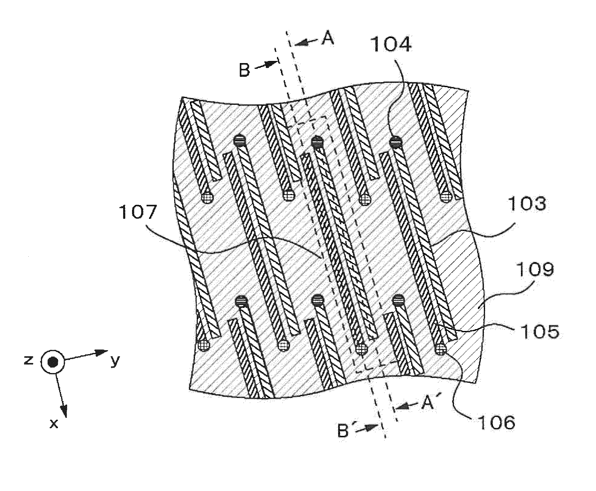
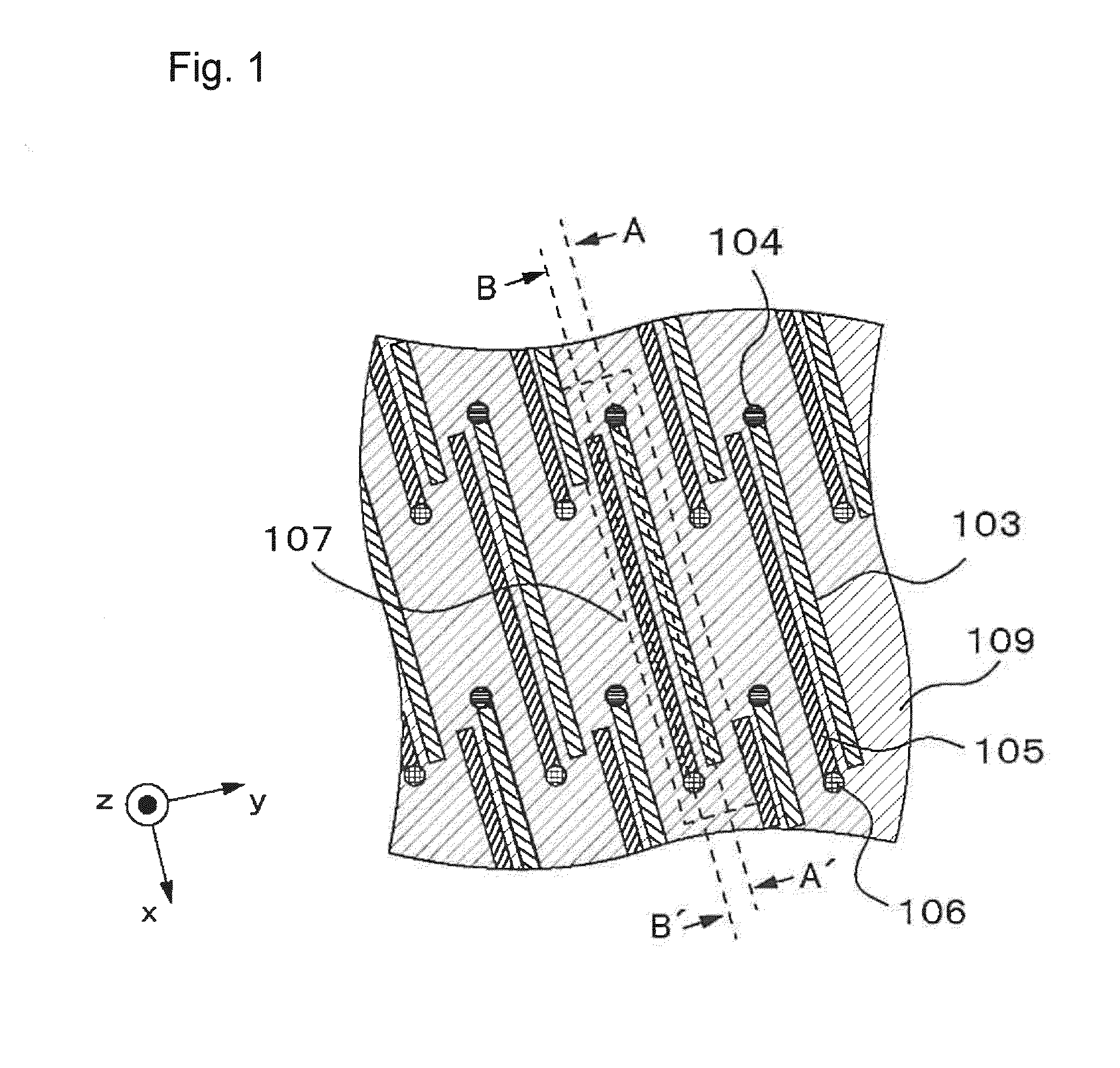
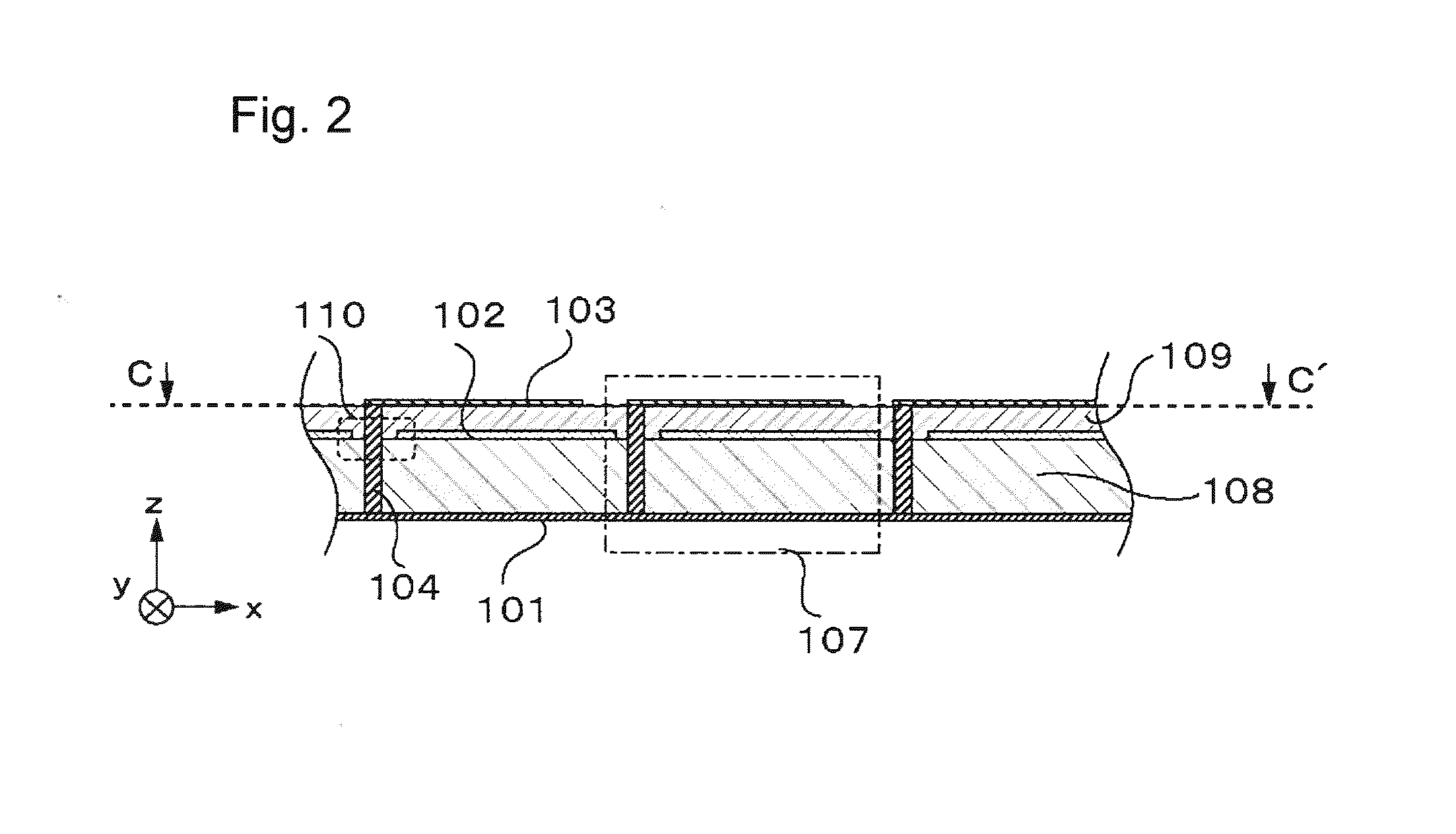
[0076]First, a description will be given of a configuration of a first exemplary embodiment of a structure according to the present invention, with reference to FIGS. 1 to 26 and FIGS. 38 and 39. Of the present exemplary embodiment, an example of a perspective view is shown in FIG. 38, an example of a plan view in FIG. 1, and examples of a cross-sectional view in FIGS. 2 and 3. FIG. 2 is a cross-sectional view taken along the line A-A′ in FIG. 1, and FIG. 3 is that taken along the line B-B′ in FIG. 1. FIG. 1 is a plan view of a plane denoted as C-C′ in FIGS. 2 and 3.
[0077]As shown in FIGS. 1 to 3, the structure of the present exemplary embodiment comprises a first conductor plane 101, a second conductor plane 102, a first transmission line 103, a first conductor via 104, a second transmission line 105 and a second conductor via 106.
[0078]The first conductor plane 101 and the second conductor plane 102 are each arranged in a different layer from that of the other. The first conductor...
second exemplary embodiment
[0115]Next, a configuration of a second exemplary embodiment of a structure according to the present invention will be described, with reference to FIGS. 27 to 30 and FIGS. 40 and 41. FIGS. 27 to 30 show examples of a cross-sectional view of a unit cell in the structure of the present exemplary embodiment. FIGS. 40 and 41 show examples of a perspective view of a unit cell in the structure of the present exemplary embodiment. The structure of the present exemplary embodiment is a modified example of the structure of the first exemplary embodiment described above, and to any constituent element which is the same as that in the above-described first exemplary embodiment, the same sign as that used in the first exemplary embodiment will be assigned, and its description will be omitted here. The present exemplary embodiment also can realize the same operation and effect as that of the first exemplary embodiment.
[0116]As shown in the cross-sectional views of FIGS. 27 and 28, the structure...
third exemplary embodiment
[0121]Next, a configuration of a third exemplary embodiment of a structure according to the present invention will be described, with reference to FIGS. 31 to 33 and FIG. 42. FIGS. 31 and 32 each show a cross-sectional view of a unit cell in a structure of the present exemplary embodiment. FIG. 42 shows an example of a perspective view of the unit cell in the structure of the present exemplary embodiment. The structure of the present exemplary embodiment is a modified example of the structure in the first exemplary embodiment described above, and to any constituent element which is the same as that in the above-described first exemplary embodiment, the same sign as that used in the first exemplary embodiment will be assigned, and its description will be omitted here. The present exemplary embodiment also can realize the same operation and effect as that in the first exemplary embodiment.
[0122]As shown in FIGS. 31, 32 and 42, the structure of the present exemplary embodiment is diffe...
PUM
 Abstract
Description
Claims
Application Information
 - R&D
- Intellectual Property
- Life Sciences
- Materials
- Tech Scout
- Unparalleled Data Quality
- Higher Quality Content
- 60% Fewer Hallucinations
Browse by: Latest US Patents, China's latest patents, Technical Efficacy Thesaurus, Application Domain, Technology Topic, Popular Technical Reports.
© 2025 PatSnap. All rights reserved.Legal|Privacy policy|Modern Slavery Act Transparency Statement|Sitemap|About US| Contact US: help@patsnap.com


