Optical Communication Module

Inactive Publication Date: 2015-10-22
HITACHI METALS LTD
View PDF7 Cites 14 Cited by
  • Summary
  • Abstract
  • Description
  • Claims
  • Application Information

AI Technical Summary

Benefits of technology

The patent aims to address the issue of high-speed digital signals losing electrical transmission during optical communication. It proposes a solution to shorten the transmission distance of digital signals between a light emitting element and a driving element inside the optical communication module to prevent signal loss and ensure reliable communication at faster speeds.

Problems solved by technology

Here, the high-speed digital signals have large loss in electrical transmission.
As a result, there is a threat that the loss of digital signals between the light emitting element and the driving element becomes too large to ignore with the increase of communication speed.

Method used


Image

  • Optical Communication Module
  • Optical Communication Module
  • Optical Communication Module

Examples


Embodiment Construction

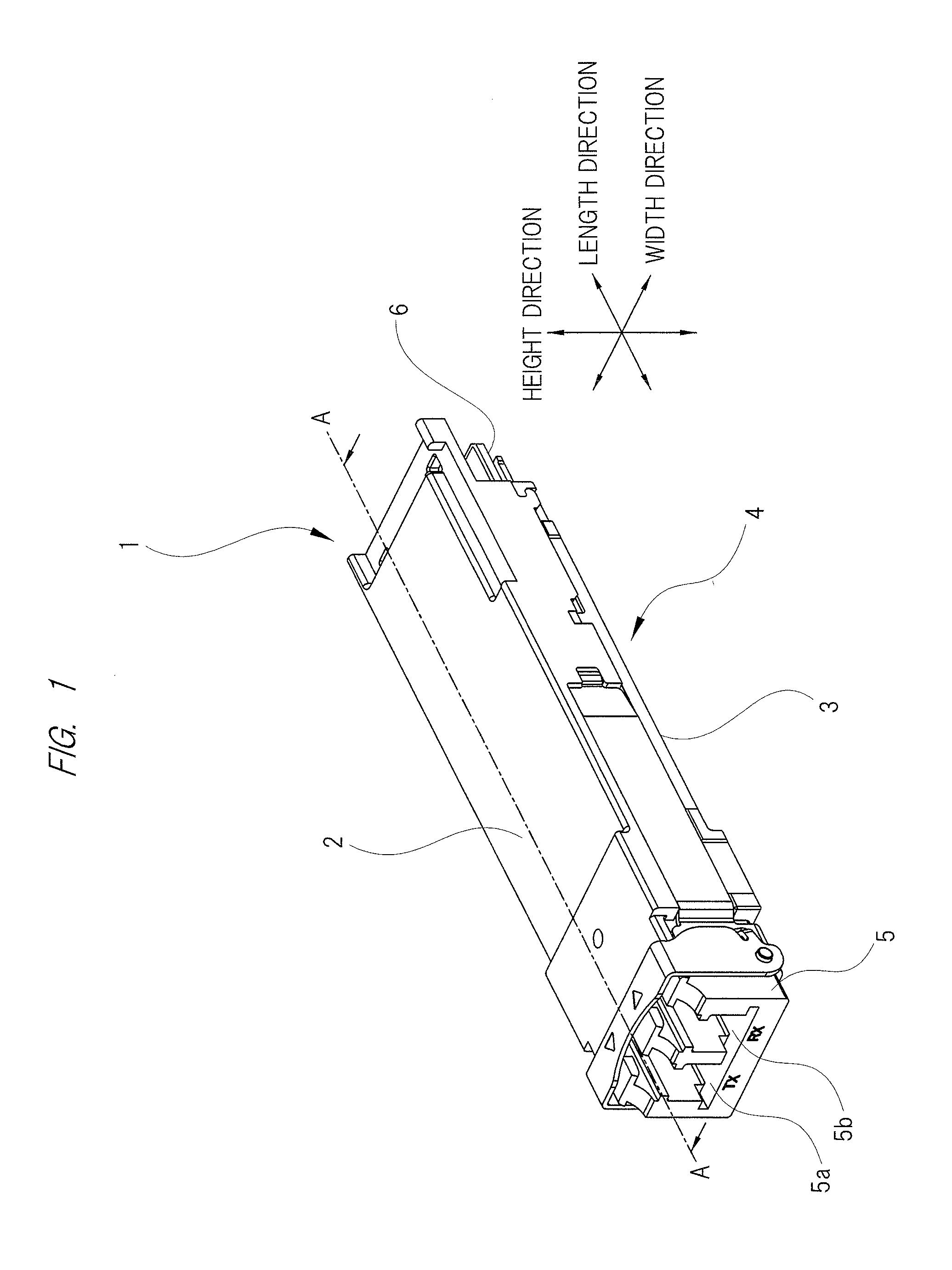
[0019]Hereinafter, an example of an optical communication module to which the present invention is applied will be described in detail with reference to accompanying drawings. The optical communication module described below is a WDM optical transceiver compliant with QSFP+ (Quad Small Form-factor Pluggable Plus) standard, and it outputs multiplexed optical signals obtained by multiplexing a plurality of optical signals having different wavelengths.

[0020]As shown in FIG. 1, an optical transceiver 1 of this embodiment has a chassis 4 made up of an upper case 2 and a lower case 3. The chassis 4 has a substantially cuboid external appearance as a whole, and has a size compliant with the QSFP+ standard. An optical adaptor 5 is provided at one longitudinal end of the chassis 4, and a card edge 6 is provided at the other longitudinal end of the chassis 4. Note that the card edge is sometimes referred to as “edge connector”. In the following description, of the both longitudinal ends of th...


PUM


Abstract

An optical communication module includes: a plurality of semiconductor lasers which emit optical signals each having different wavelengths; a plurality of driver ICs which drive each of the plurality of semiconductor lasers; and a substrate on which both of the semiconductor lasers and the driver ICs are mounted. The semiconductor lasers are mounted on a first surface of the substrate and the driver ICs are mounted on a second surface of the substrate opposite to the first surface.

Description

CROSS-REFERENCE TO RELATED APPLICATION[0001]The present application claims priority from Japanese Patent Application No. 2014-085359 filed on Apr. 17, 2014, the content of which is hereby incorporated by reference into this application.TECHNICAL FIELD OF THE INVENTION[0002]The present invention relates to an optical communication module, in particular, to an optical communication module used for the wavelength division multiplexing (WDM) communication.BACKGROUND OF THE INVENTION[0003]Various types of WDM optical communication modules have been developed, and a WDM optical transceiver is one of them. For example, a WDM optical transceiver provided with a transmitter optical sub-assembly (TOSA) which multiplexes a plurality of optical signals emitted from a plurality of light sources and having different wavelengths has been developed and put into practical use.[0004]A conventional transmitter optical sub-assembly has a plurality of light emitting elements which output optical signals...

Claims


Application Information

Patent Timeline
IPC IPC(8): F21V23/00
CPCF21V23/005G02B6/4262G02B6/428G02B6/4215G02B6/4268G02B6/4274G02B6/4284
Inventor TAMURA, KENICHITAKAHASHI, RYUTASUNAGA, YOSHINORI
Owner HITACHI METALS LTD
Why Eureka
Try Eureka