Light emitting element and method of manufacturing the same

a technology of light-emitting elements and manufacturing methods, which is applied in the direction of semiconductor/solid-state device manufacturing, electrical equipment, semiconductor devices, etc., can solve the problems of affecting the production efficiency of light-emitting elements, etc., to achieve the effect of improving productivity

Active Publication Date: 2015-10-01
TOYODA GOSEI CO LTD
View PDF6 Cites 12 Cited by
  • Summary
  • Abstract
  • Description
  • Claims
  • Application Information

AI Technical Summary

Benefits of technology

[0069]In the fifth aspect, it is possible to improve productivity, as compared to a method of dividing each of the light emitting elements from the wafer of the crystal growth substrate and then forming the irregularities on the second surface of the crystal growth substrate.

Problems solved by technology

However, this method has a problem of low productivity because it takes a lot of man-hours.
Accordingly, the load from the breaking blade is not properly applied to a dividing line portion of the crystal growth substrate.
Consequently, there is a problem that separation failure (dividing failure) is liable to occur.
However, the separation failure is liable to occur especially in the thinned gallium nitride substrate.
Further, the thinned gallium nitride substrate is liable to be damaged.
Accordingly, there is also a problem that the handling such as the tape transfer is difficult to perform.
However, the adhesion of the wafer fixing tape is damaged when irregularities are formed on one surface of the crystal growth substrate.
Accordingly, there is a problem that the light emitting element is liable to be separated from the wafer fixing tape.
However, the absorption is deteriorated when the irregularities are formed on one surface of the crystal growth substrate.
Accordingly, there is a problem that the light emitting element is liable to be separated from the collet.
However, in this case, there is a problem that the irregularities are liable to be damaged by the application of the load when the irregularities are formed on one surface of the crystal growth substrate.

Method used


Image

  • Light emitting element and method of manufacturing the same
  • Light emitting element and method of manufacturing the same
  • Light emitting element and method of manufacturing the same

Examples


first embodiment

Operation / Effect of First Embodiment

[0104]According to the first embodiment, the following operation / effects can be obtained.

[1-1]

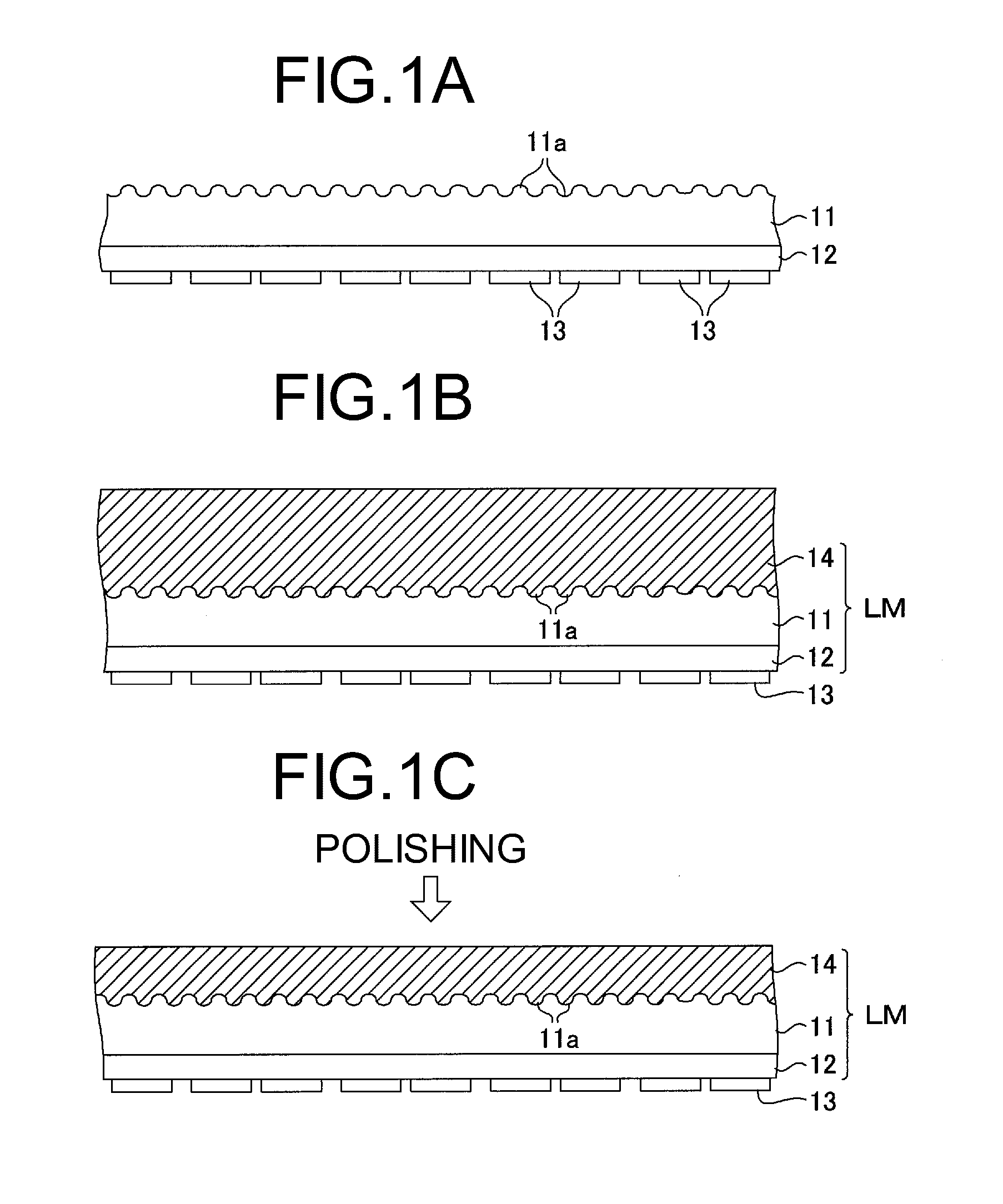
[0105]Since the light generated in the semiconductor layer 12 is diffused in the irregularities 11a on the second surface of the crystal growth substrate 11, it is possible to suppress the multiple reflections on the inside of the light emitting element 10. Accordingly, the light extraction efficiency of the light emitting element 10 can be improved.

[0106]Further, when the irregularities 11a are formed on the second surface of the crystal growth substrate 11, the reflectivity of the light that is generated in the semiconductor layer 12 and incident on the second surface is lowered. Accordingly, it is possible to increase the light transmittance, so that the light extraction efficiency of the light emitting element 10 can be improved.

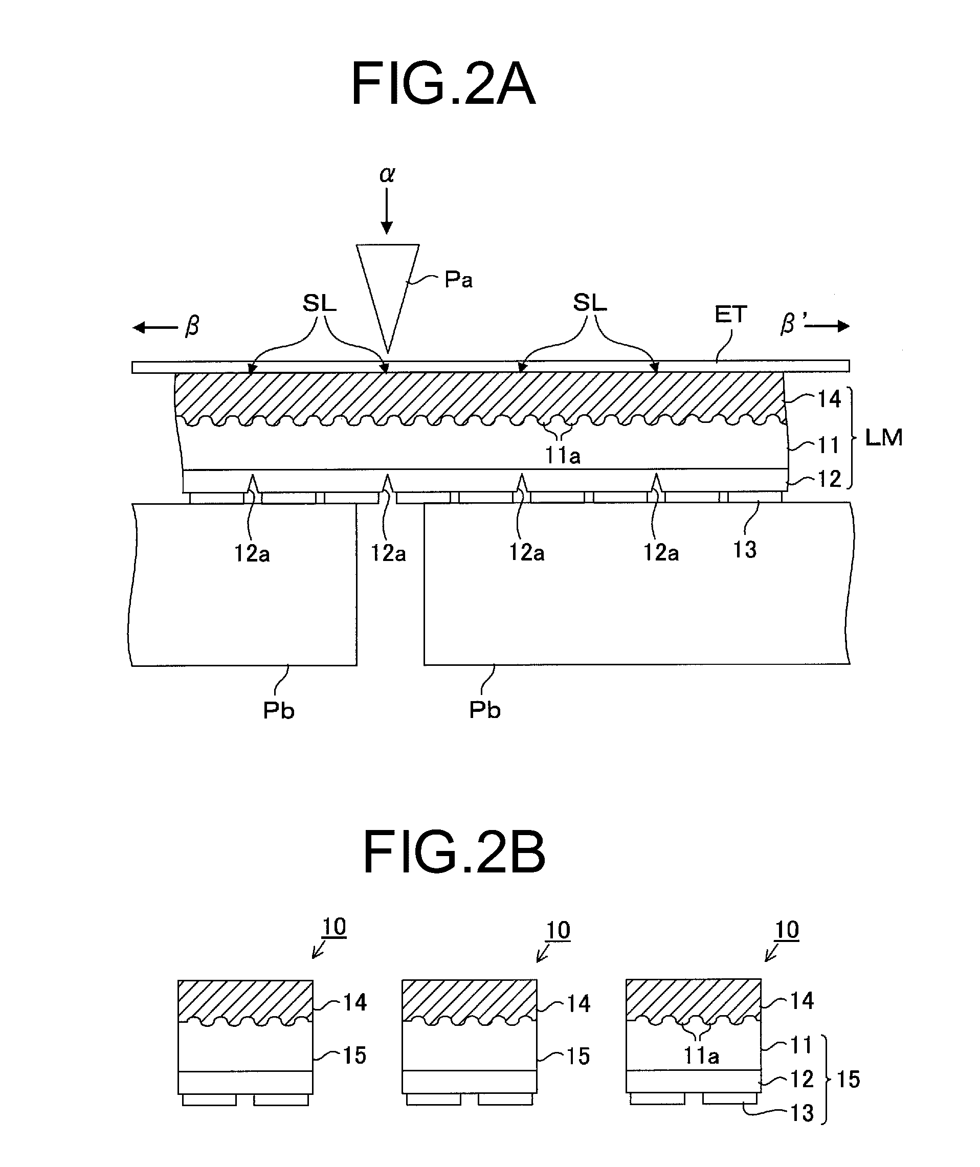
[0107]As shown in FIG. 2B, when dividing the wafer of the stacked crystal growth substrate 11, the semiconductor layer 12 an...

second embodiment

Operation / Effect of Second Embodiment

[0131]According to the second embodiment, the following operation / effects can be obtained, in addition to the above operation / effects of the first embodiment.

[2-1]

[0132]In the light emitting element 10 of the second embodiment, the protective layer 14 functions as a luminescent color conversion member (wavelength conversion member or phosphor layer). Further, a primary light (blue light) is an excitation light emitted from the LED chips 15 and a portion of the primary light is excited by phosphors in the protective layer 14 to generate a luminescent color-converted (wavelength-converted) secondary light (yellow light). The primary light and the secondary light are mixed to generate a mixed-color light (white light). The mixed-color light is emitted to the outside through the protective layer 14.

[0133]Therefore, light energy that is not converted during the luminescent color conversion becomes thermal energy to cause the phosphors to generate heat...

third embodiment

[0166]A light emitting element 10 of a third embodiment is different from the light emitting element of the first embodiment in that the protective layer 14 includes a light scattering material (e.g., silica, titanium oxide, etc.) for scattering the emitted light of the LED chips 15.

[0167]In the third embodiment, the protective layer 14 containing the light scattering material functions as a light scattering member and the light incident on the protective layer 14 from the crystal growth substrate 11 is scattered by the light scattering material in the protective layer 14. Accordingly, in addition to the above operation / effects of the first embodiment, it is possible to suppress the multiple reflections on the inside of the protective layer 14, so that the light extraction efficiency of the light emitting element 10 can be further improved.

[0168]Meanwhile, the protective layer 14 may be formed by a translucent material in which voids (bubbles) for scattering the emitted light of the...


PUM

PropertyMeasurementUnit
particle sizeaaaaaaaaaa

Abstract

A light emitting element includes a crystal growth substrate formed in a flat shape and that has a translucency, a semiconductor layer that constitutes a light emitting element structure and is formed at a side of a first surface of the crystal growth substrate, irregularities formed on a second surface of the crystal growth substrate, the second surface being an opposite surface of the first surface, and a protective layer that has a translucency and a predetermined hardness and brittleness, and covers the irregularities formed on the second surface of the crystal growth substrate.

Description

CROSS REFERENCE TO RELATED APPLICATIONS[0001]This application claims the benefit of Japanese Patent Application (No. P2014-069842) filed on Mar. 28, 2014, the entire contents of which are incorporated herein by reference.BACKGROUND OF THE INVENTION[0002]1. Field of the Invention[0003]The present invention relates to a light emitting element and a method of manufacturing the same. More particularly, the present invention relates to a light emitting element where irregularities are formed on one surface of a crystal growth substrate, and a method of manufacturing the same.[0004]2. Description of the Related Art[0005]Patent Document 1 discloses a nitride-based LED where a light emitting structure made of a nitride semiconductor is provided on a front surface of a nitride semiconductor substrate. Here, a roughened region is provided on a back surface of the nitride semiconductor substrate. The roughened region is provided with a plurality of protrusions. The light generated in the light...

Claims


Application Information

Patent Timeline
Patent Type & Authority Applications(United States)
IPC IPC(8): H01L33/22H01L33/56H01L33/58
CPCH01L33/22H01L33/56H01L33/58H01L33/0095H01L33/44H01L33/501H01L2933/0041
Inventor WADA, SATOSHI
Owner TOYODA GOSEI CO LTD
Why Eureka
Try Eureka