Light emitting device and method of manufacturing same
a technology of light-emitting devices and manufacturing methods, which is applied in the manufacture of semiconductor/solid-state devices, semiconductor devices, electrical devices, etc., to achieve the effect of improving the optical output of the light-emitting device and suppressing the light absorption by the substra
- Summary
- Abstract
- Description
- Claims
- Application Information
AI Technical Summary
Benefits of technology
Problems solved by technology
Method used
Image
Examples
first embodiment
Light-Emitting Device 100
[0019]FIG. 1A is a schematic plan view of a light-emitting device according to a first embodiment and FIG. 1B is a diagram showing a section A-A in FIG. 1A.
[0020]As shown in FIGS. 1A and 1B, a light-emitting device 100 according to the first embodiment includes a substrate 10, a light-emitting element 20 mounted on the substrate 10, a first light-transmissive member 40 bonded to an upper surface of the light-emitting element 20 via an adhesive 30, and a second light-transmissive member 50 placed on an upper surface of the first light-transmissive member 40. A peripheral edge of a lower surface of the first light-transmissive member 40 is positioned more inward than a peripheral edge of the upper surface of the light-emitting element 20 in a plan view, and the adhesive 30 is provided so as to extend from the upper surface of the light-emitting element 20 to a lower surface of the second light-transmissive member 50 while covering a side surface of the first l...
second embodiment
[0052][Light-Emitting Device 200 ]
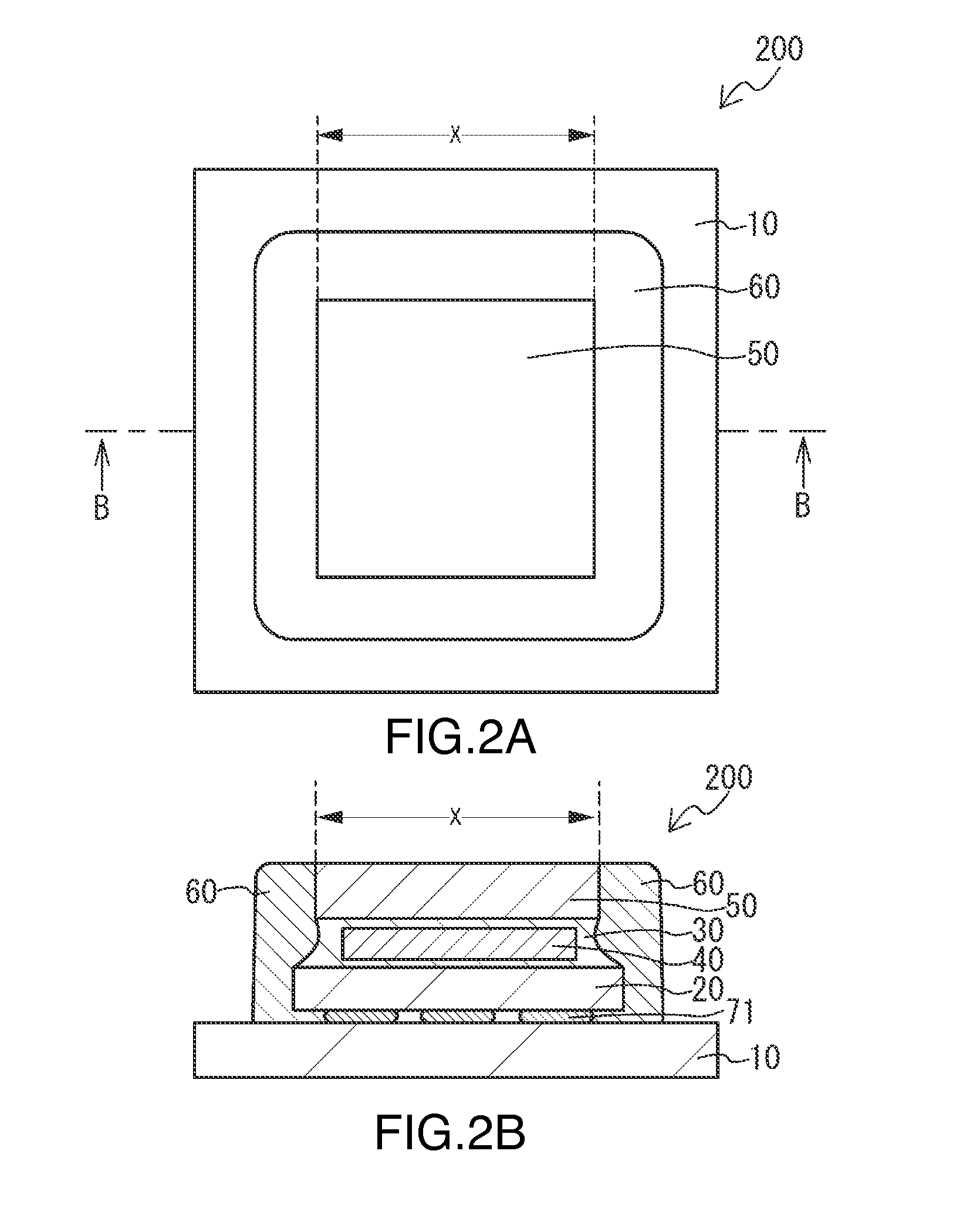
[0053]FIG. 2A is a schematic plan view of a light-emitting device according to a second embodiment and FIG. 2B is a diagram showing a section B-B in FIG. 2A.
[0054]As shown in FIGS. 2A and 2B, the light-emitting device 200 according to the second embodiment is a light-emitting device in which the peripheral edge of the lower surface of the second light-transmissive member 50 is positioned more inward than the peripheral edge of the upper surface of the light-emitting element 20 in a plan view, while the light-emitting device 100 according to the first embodiment is a light-emitting device in which the lower surface of the second light-transmissive member 50 has a same shape as the light-emitting element 20 in a plan view. With the light-emitting device 200 according to the second embodiment, absorption of light by the substrate 10 can be suppressed and optical output of the light-emitting device can be improved in a similar manner to the light-emitti...
third embodiment
[0059][Light-Emitting Device 300 ]
[0060]FIG. 3A is a schematic plan view of a light-emitting device according to a third embodiment and FIG. 3B is a diagram showing a section C-C in FIG. 3A.
[0061]As shown in FIGS. 3A and 3B, the light-emitting device 300 according to the third embodiment is a light-emitting device in which the peripheral edge of the lower surface of the second light-transmissive member 50 is positioned more outward than the peripheral edge of the upper surface of the light-emitting element 20 in a plan view, while the light-emitting device 100 according to the first embodiment is a light-emitting device in which the lower surface of the second light-transmissive member 50 has a same shape as the light-emitting element 20 in a plan view. With the light-emitting device 300 according to the third embodiment, absorption of light by the substrate 10 can be suppressed and optical output of the light-emitting device can be improved as well as the light-emitting device 100 ...
PUM
 Abstract
Description
Claims
Application Information
 - Generate Ideas
- Intellectual Property
- Life Sciences
- Materials
- Tech Scout
- Unparalleled Data Quality
- Higher Quality Content
- 60% Fewer Hallucinations
Browse by: Latest US Patents, China's latest patents, Technical Efficacy Thesaurus, Application Domain, Technology Topic, Popular Technical Reports.
© 2025 PatSnap. All rights reserved.Legal|Privacy policy|Modern Slavery Act Transparency Statement|Sitemap|About US| Contact US: help@patsnap.com


