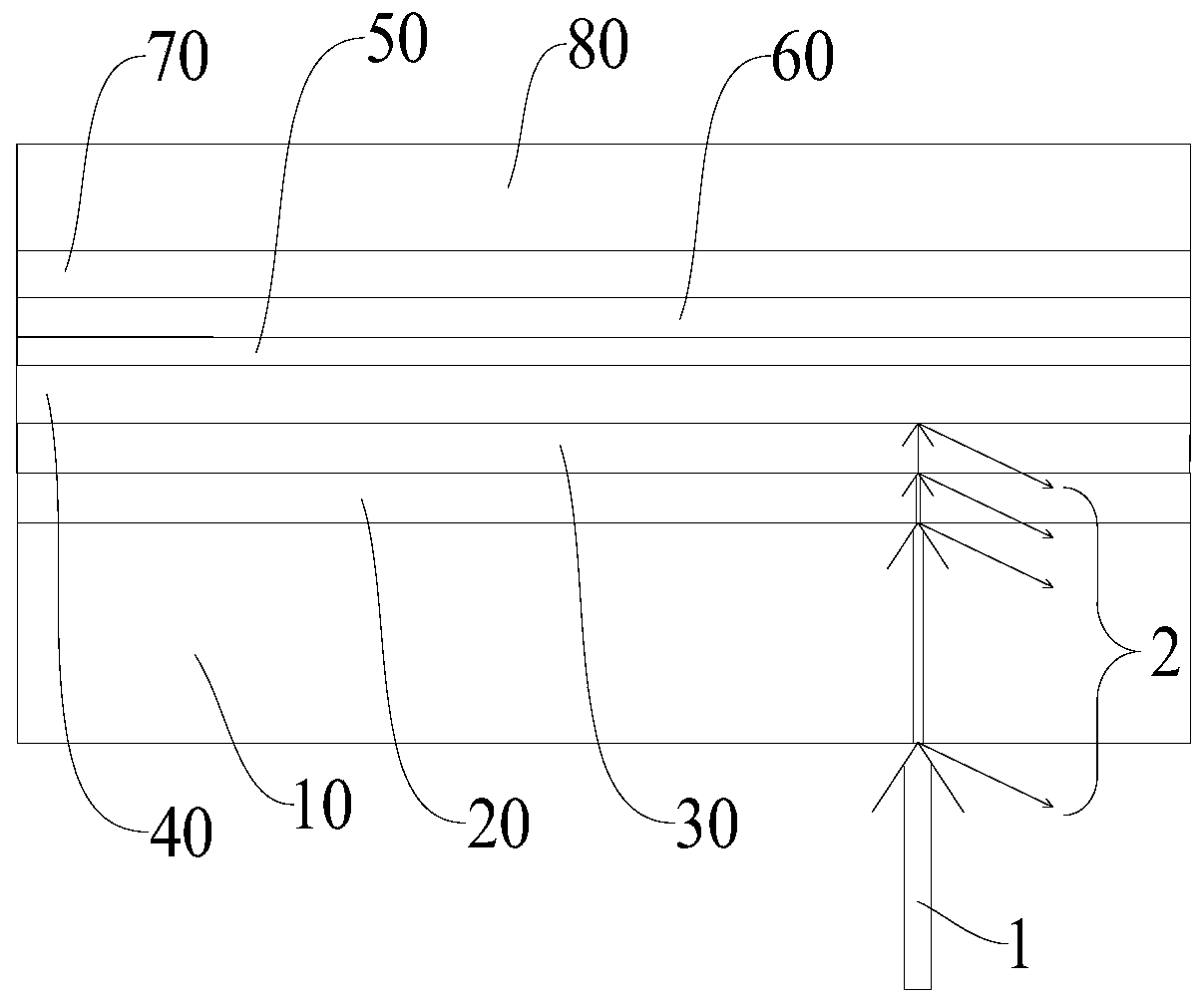
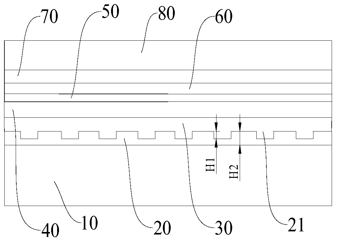
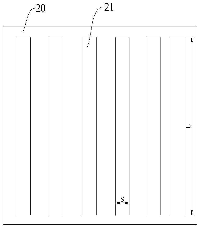
Thin film solar cells and preparation methods thereof
A technology of solar cells and thin films, applied in the field of solar cells, can solve the problems of low energy conversion efficiency of solar cells and the like
- Summary
- Abstract
- Description
- Claims
- Application Information
AI Technical Summary
Problems solved by technology
Method used
Image
Examples
Embodiment 1
[0056] Test sample: Indium tin oxide (ITO) transparent electrodes with a thickness of 50 nm and 500 nm were respectively formed on the surface of a glass transparent substrate to obtain a test sample.
[0057] Test method: test the light absorption performance of the above test samples under the condition of AM1.5G, see the test results and AM1.5G spectral irradiance distribution Figure 9 .
[0058] Figure 9 The spectral irradiance distribution of AM1.5G and the absorption characteristics of the ITO transparent electrode are shown as a function of wavelength and thickness of the transparent electrode. Depend on Figure 9It can be seen that when the wavelength is less than 450nm, the light absorptivity increases significantly with the increase of the thickness of the transparent electrode, and the light absorptivity decreases sharply with the increase of the wavelength. When the wavelength increases further, the light absorptivity increases with the increase of the waveleng...
Embodiment 2
[0060] Test sample: The test sample is a plurality of solar cells, the solar cell includes a glass transparent substrate, an ITO transparent electrode, an electron transport layer (titanium dioxide), a perovskite light-absorbing layer, a hole transport layer (Spiro-OMeTAD) and The silver electrode and the ITO transparent electrode in multiple solar cells have different thicknesses, which are 0nm (ie, not including the ITO transparent electrode), 100nm, 200nm, 300nm, 400nm and 500nm.
[0061] Test method: For the above-mentioned multiple solar cells, the photogenerated current loss caused by the reflection of the transparent electrode layer with different thicknesses and the photogenerated current loss caused by the light absorption of the transparent electrode are simulated and calculated according to the conventional basic logic method in this field. The test results are shown in Figure 10 .
[0062] Figure 10 The test results of the photogenerated current loss due to the ...
Embodiment 3
[0064] Test sample: ITO transparent electrode (thickness: 500nm), electron transport layer (titanium dioxide, thickness: 40nm), perovskite light-absorbing layer (MAPbI) are sequentially formed on the glass transparent substrate 3 , thickness is 500nm), hole transport layer (Spiro-OMeTAD, thickness is 150nm), metal electrode (silver, thickness is 100nm), encapsulation layer (ethylene-vinyl acetate copolymer, EVA) and backplane (glass), get The test sample, wherein, the step of forming the ITO transparent electrode is: forming a transparent conductive layer on a transparent substrate; using a laser to form a plurality of grooves arranged at intervals on the transparent conductive layer to obtain a transparent electrode. A series of solar cells with different aperture ratios (groove area / total area of transparent electrodes) and thicknesses of the transparent electrodes at the bottom of the grooves were prepared by using the above method.
[0065] Test method: For the above ser...
PUM
| Property | Measurement | Unit |
|---|---|---|
| Thickness | aaaaa | aaaaa |
| Thickness | aaaaa | aaaaa |
| Thickness | aaaaa | aaaaa |
Abstract
Description
Claims
Application Information
 - R&D
- Intellectual Property
- Life Sciences
- Materials
- Tech Scout
- Unparalleled Data Quality
- Higher Quality Content
- 60% Fewer Hallucinations
Browse by: Latest US Patents, China's latest patents, Technical Efficacy Thesaurus, Application Domain, Technology Topic, Popular Technical Reports.
© 2025 PatSnap. All rights reserved.Legal|Privacy policy|Modern Slavery Act Transparency Statement|Sitemap|About US| Contact US: help@patsnap.com


