Pixel structure and liquid crystal panel
a liquid crystal panel and pixel technology, applied in the field of pixel structure and liquid crystal panel, can solve the problems of increasing power consumption, affecting the thickness of the dielectric layer, and affecting the capacitive load between the common electrode and the data line, so as to improve the lc efficiency and increase the capacitive load
- Summary
- Abstract
- Description
- Claims
- Application Information
AI Technical Summary
Benefits of technology
Problems solved by technology
Method used
Image

Examples
first embodiment
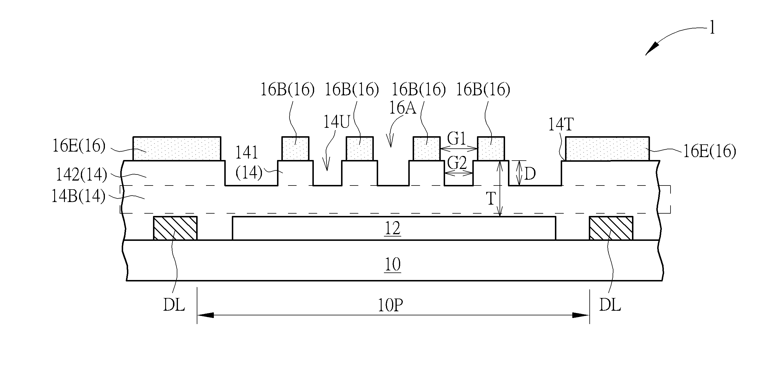
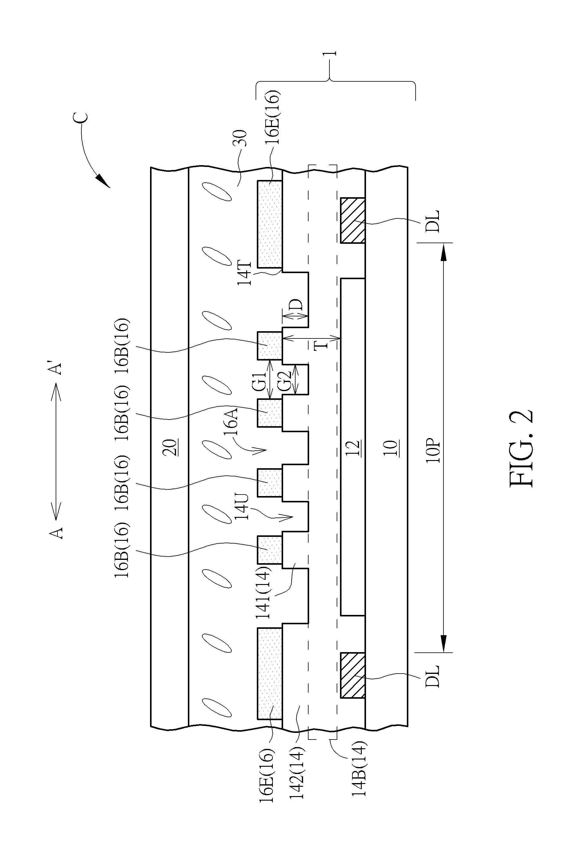
[0028]Refer to FIG. 1 and FIG. 2. FIG. 1 is a top view of a pixel structure according to the present invention, and FIG. 2 is a cross-sectional view of the pixel structure of FIG. 1 along line A-A′. In this embodiment, a pixel structure of an FFS LCD panel is used as an example, but not a limitation. The pixel structure of the present embodiment may be applied in other suitable display panels. As shown in FIG. 1 and FIG. 2, the pixel structure 1 of this embodiment includes a substrate 10, a plurality of gate line GL, a plurality of data lines DL and a plurality of pixels P. The substrate 10 may include a transparent substrate e.g. a glass substrate, a plastic substrate or a quartz substrate, but not limited thereto. The substrate 10 may be various types of rigid substrates or flexible substrates. The gate lines GL and the data lines DL are intersected, defining a plurality of pixel regions 10P (also referred to as sub-pixel regions). The pixels P (also referred to sub-pixels) are di...
third embodiment
[0043]Refer to FIG. 9 and FIG. 10. FIG. 9 is a top view of a pixel structure according to the present invention, and FIG. 10 is a cross-sectional view of the pixel structure of FIG. 9 along line D-D′. As shown in FIG. 9 and FIG. 10, in the pixel structure 3 of this embodiment, there is only one first island structure 141, and the first island structure 141 and the second island structure 142 disposed on the base structure 14B form the cavity 14U. The thickness sum T of the base structure 14B and the first island structure 141 is greater than the depth D of the cavity 14U. The branch electrodes 16B are disposed on the top surface 14T of the first island structure 141 and partially expose the top surface 14T of the first island structure 141, and the second island structure 142 overlaps the corresponding data line DL. The second electrode 16 may further include a fringe electrode 16E disposed on the top surface 14T of the second island structure 142. The fringe electrode 16E may be el...
fifth embodiment
[0046]Refer to FIGS. 12-14. FIG. 12 is a top view of a pixel structure according to the present invention, FIG. 13 is a cross-sectional view of the pixel structure of FIG. 12 along line E-E′ and FIG. 14 is a cross-sectional view of the pixel structure of FIG. 12 along line F-F′. As shown in FIG. 12, the pixel structure 5 of this embodiment includes at least one first pixel P1 and at least one second pixel P2. As shown in FIG. 13, the first pixel P1 includes a first electrode 12, a first dielectric layer 14 and a second electrode 16. The first electrode 12 is disposed on the substrate 10, and electrically connected to the corresponding data line DL. The first dielectric layer 14 is disposed on the first electrode 12, where the first dielectric layer 14 has at least one first island structure 141, a base structure 14B and at least one second island structure 142, and the first island structure 141 and the second island structure 142 disposed on the base structure 14B form a plurality ...
PUM
 Abstract
Description
Claims
Application Information
 - R&D
- Intellectual Property
- Life Sciences
- Materials
- Tech Scout
- Unparalleled Data Quality
- Higher Quality Content
- 60% Fewer Hallucinations
Browse by: Latest US Patents, China's latest patents, Technical Efficacy Thesaurus, Application Domain, Technology Topic, Popular Technical Reports.
© 2025 PatSnap. All rights reserved.Legal|Privacy policy|Modern Slavery Act Transparency Statement|Sitemap|About US| Contact US: help@patsnap.com