Composition for manufacturing integrated circuit devices, optical devices, micromachines and mechanical precision devices
a technology micromachines, applied in the field of composition for manufacturing integrated circuit devices, optical devices, micromachines and mechanical precision devices, can solve the problems of poor adhesion of patterned structures to the underlayer, swelling and weakening of structures, and achieve the effects of reducing diffusion, preventing swelling of the photoresist layer, and reducing the surface tension of the developer composition
- Summary
- Abstract
- Description
- Claims
- Application Information
AI Technical Summary
Benefits of technology
Problems solved by technology
Method used
Image
Examples
example 1
[0107]Photoresist layers having features with line-space structures and line-width of 26 nm (feature dimension) and an aspect ratio of about 4 were developed using a developer composition comprising trimethyladamantylammonium hydroxide (D1). The space between the photoresist lines was 52 nm.
[0108]Silicon wafers were provided with 100 nm thick layers of an immersion photoresist. The photoresist layers were exposed to UV radiation of a wavelength of 193 through a mask using ultrapure water as the immersion liquid. Thereafter, the exposed photoresist layers were baked and developed with an aqueous developer solution containing 0.26 N of D1. The baked and developed photoresist layers were subjected to a chemical rinse treatment using a chemical rinse solution containing tetramethylammonium hydroxide (TMAH).
[0109]The chemical rinse solution was applied on the wafer as a puddle. Thereafter, the silicon wafers were spun dry.
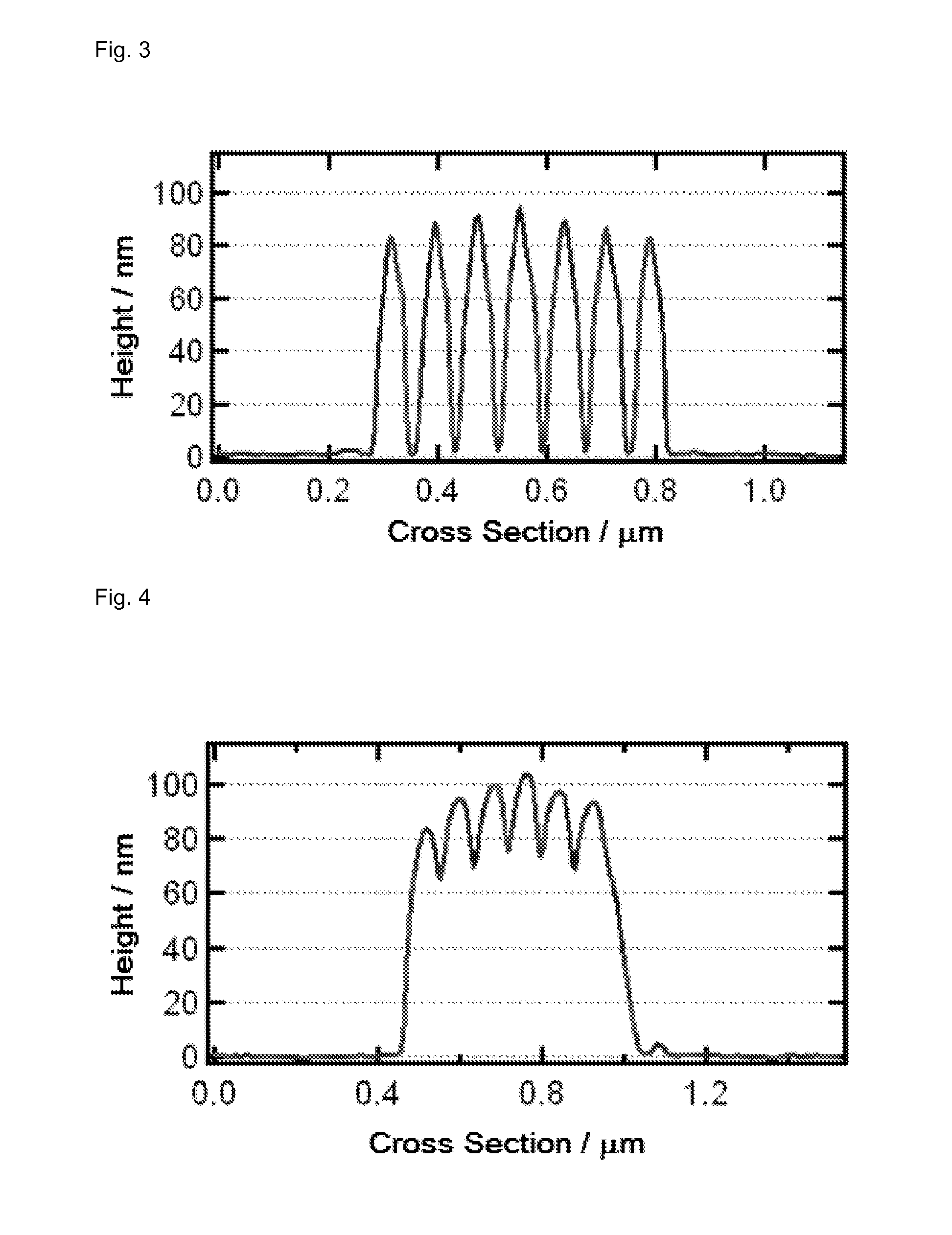
[0110]FIG. 3 shows the respective height profile measured by AFM a...
example 3
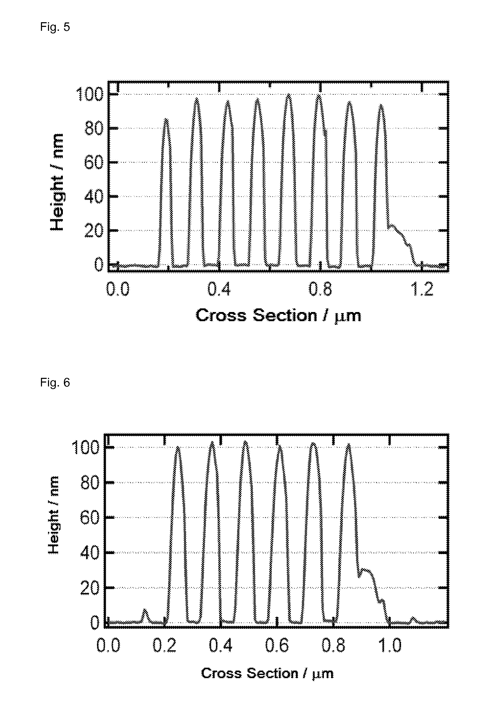
[0113]Example 1 was repeated except that 0.26 N dimethyldicyclohexylammonium hydroxide (D2) was used instead of surfactant D1 in the photoresist developer solution and the line width was 40 nm and the space between the photoresist lines was 80 nm.
[0114]FIG. 5 shows the respective height profile measured by AFM after development with D2 and rinse treatment. The dried patterned photoresist layers having photoresist line-width dimensions of 40 nm and an aspect ratio of about 2.5 did not show any pattern collapse. The deep trenches in the photoresist indicate a low swelling of the photoresist.
PUM
| Property | Measurement | Unit |
|---|---|---|
| pH | aaaaa | aaaaa |
| aspect ratio | aaaaa | aaaaa |
| thickness | aaaaa | aaaaa |
Abstract
Description
Claims
Application Information
 - R&D
- Intellectual Property
- Life Sciences
- Materials
- Tech Scout
- Unparalleled Data Quality
- Higher Quality Content
- 60% Fewer Hallucinations
Browse by: Latest US Patents, China's latest patents, Technical Efficacy Thesaurus, Application Domain, Technology Topic, Popular Technical Reports.
© 2025 PatSnap. All rights reserved.Legal|Privacy policy|Modern Slavery Act Transparency Statement|Sitemap|About US| Contact US: help@patsnap.com


