Method of Designing Semiconductor Device, Designing Assistance Program, Designing Apparatus, and Semiconductor Device

a semiconductor device and assistance program technology, applied in the direction of cad circuit design, error detection/correction, instruments, etc., can solve the problem that the consumption power cannot be reduced to the real minimum consumption power, and achieve the effect of reducing consumption energy

Inactive Publication Date: 2015-06-11
RENESAS ELECTRONICS CORP
View PDF5 Cites 6 Cited by
  • Summary
  • Abstract
  • Description
  • Claims
  • Application Information

AI Technical Summary

Benefits of technology

[0011]However, as a result of examination of the inventors of the present invention, it was found out that the consumption power cannot be reduced to the real minimum consumption power by the conventional minimum operating frequency and minimum operating voltage. In the conventional DVFS control, during the time T in which the process is executed, the operating frequency is kept constant at the lowest operating frequency f and the operating voltage is maintained constant at the lowest voltage operating voltage V, and the consumption power is reduced. By further subdividing the process and performing the DVFS control in a unit of finer time, it is expected that the consumption power can be more reduced. In this method, however, the lowest operating frequency and the lowest operating voltage have to be calculated for each subdivided time, and the subdivision is limited to suppress the calculation amount to an amount which is allowed in reality. Consequently, by the conventional DVFS control, consumption power cannot be reduced to the real minimum consumption power.

Problems solved by technology

In this method, however, the lowest operating frequency and the lowest operating voltage have to be calculated for each subdivided time, and the subdivision is limited to suppress the calculation amount to an amount which is allowed in reality.
Consequently, by the conventional DVFS control, consumption power cannot be reduced to the real minimum consumption power.

Method used


Image

  • Method of Designing Semiconductor Device, Designing Assistance Program, Designing Apparatus, and Semiconductor Device
  • Method of Designing Semiconductor Device, Designing Assistance Program, Designing Apparatus, and Semiconductor Device
  • Method of Designing Semiconductor Device, Designing Assistance Program, Designing Apparatus, and Semiconductor Device

Examples


first embodiment

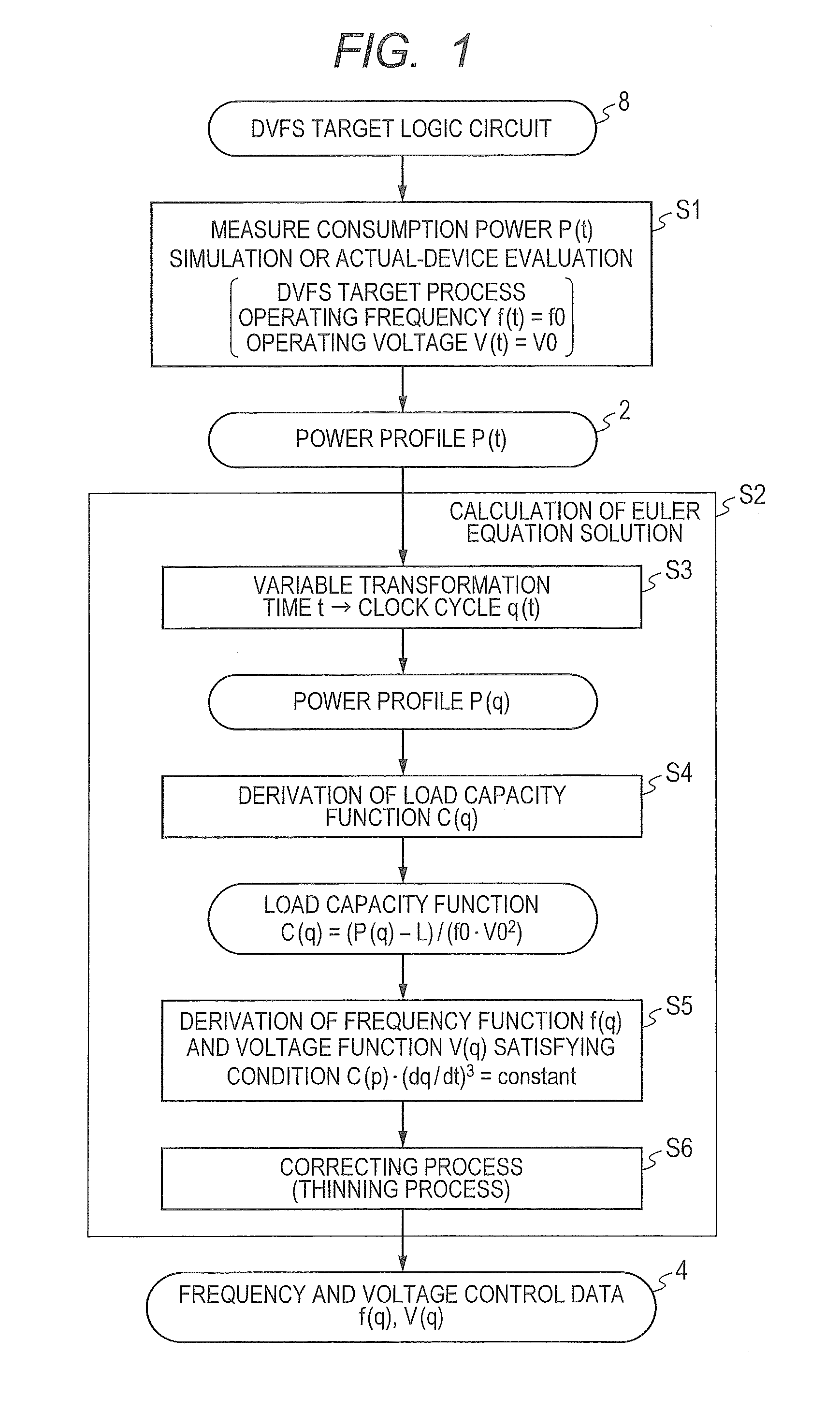
[0092]DVFS Control Based on Euler Equation Solution According to Calculus of Variations

Algorithm

[0093]The principle that an ideal DVS control in which consumption energy is theoretically minimized can be executed by the above-described representative embodiment will be described specifically.

[0094]Generally, when consumption power is expressed as P, consumption energy (power amount) is expressed as E, and time is expressed as t, the following integral equation is satisfied with respect to E.

E=∫Pdt  Equation 2

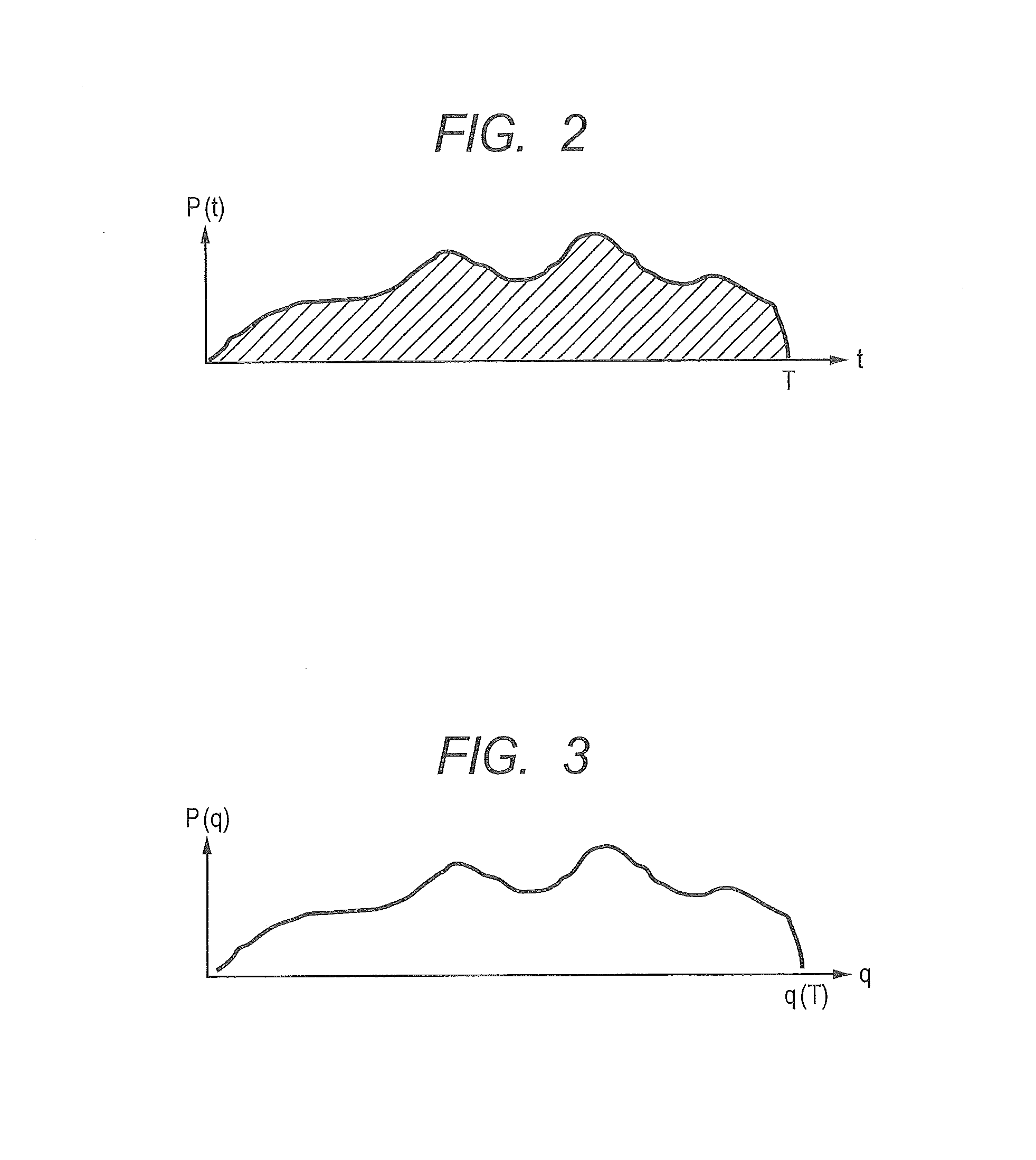
[0095]FIG. 2 is a graph illustrating time fluctuations of the consumption power P when a DVFS control target circuit (logic circuit) 8 is operated at the constant frequency f in DVFS control. In the actual logic circuit 8, even in the case of performing an operation while maintaining a period of executing a target process and an operating frequency to be constant, the consumption power P fluctuates with time as illustrated in FIG. 2.

[0096]The reason why P fluctuates with time ev...

second embodiment

Processor for Including Control Data into Program

[0136]FIG. 8 is an explanatory diagram expressing an example of applying a method of designing a semiconductor device according to a second embodiment.

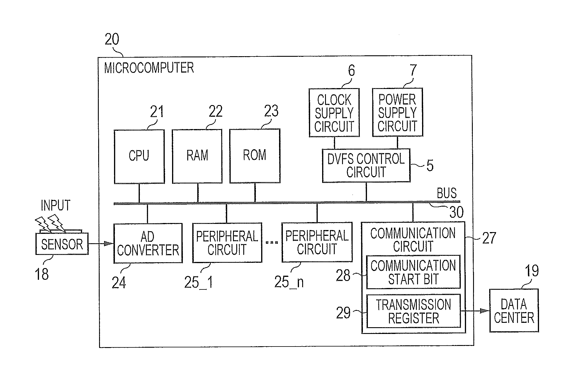
[0137]A semiconductor device 100 is configured by having the DVFS control target circuit 8, the DVFS control circuit 5, the clock supply circuit 6, and the power supply circuit 7. The DVFS control circuit 5 has a frequency control register 13 and a voltage control register 14. To the DVFS control target circuit 8, the clock supply circuit 6 supplies an operation clock of a frequency designated by the frequency control register 13 and the power supply circuit 7 supplies power of an operating voltage designated by the voltage control register 14. The DVFS control target circuit 8 has a processor such as a CPU (Central Processing Unit) or the like having a code memory 16 in which a program is stored, and can write data to the frequency control register 13 and the voltage control register 1...

third embodiment

Dedicated Hardware Holding Control Data in Storing Device

[0150]FIG. 13 is an explanatory diagram expressing an example of applying a method of designing a semiconductor device according to a third embodiment.

[0151]In a method of designing the semiconductor device 100 according to the third embodiment, in a manner similar to the embodiment illustrated in FIG. 7, the power profile information 2 is obtained by a simulation tool for the DVFS target circuit 8 or the actual device evaluation environment 1. At this time, a program stored in the code memory 16 is executed by the processor of the DVFS target circuit 8 at a predetermined clock frequency. Using the data of the power profile information 2 obtained, by the calculation tool 3 of the Euler equation solution, the frequency / voltage control data 4 based on the Euler equation solution is obtained. Since the operating frequency and the operating voltage optimum for each of the clock cycles are specified in the frequency / voltage control...


PUM


Abstract

The present invention provides a method of designing a semiconductor device capable of executing a DVFS control which minimizes consumption energy. A consumption power profile P(t) when a known operating voltage and a clock of a known frequency are given to a logic circuit as a DVFS target and a process as a DVFS target is executed is obtained. The obtained power profile is converted to a function related to a clock cycle q(t), and a load capacity of the target logic circuit is obtained as a function of the clock cycle q(t). An operating voltage and an operating frequency are calculated as functions (V(q), f(q)) for a clock cycle so as to satisfy a condition using, as a constant, a product (C(q)·(dq / dt){circle around ( )}3) of the load capacity function and cube of time differentiation of the clock cycle. The calculated functions of the operating voltage and the operating frequency are solutions of the Euler equation according to the calculus of variations, and consumption energy is minimized.

Description

CROSS-REFERENCE TO RELATED APPLICATIONS[0001]The disclosure of Japanese Patent Application No. 2013-252039 filed on Dec. 5, 2013 including the specification, drawings and abstract is incorporated herein by reference in its entirety.BACKGROUND[0002]The present invention relates to a method of designing a semiconductor device, a designing assistance program, a designing apparatus, and a semiconductor device and, more particularly, can be suitably used for a semiconductor device whose consumption power can be reduced by dynamically controlling an operating frequency and an operating voltage.[0003]There is a known technique which reduces consumption power of a semiconductor device, particularly, a CMOS (Complementary Metal Oxide Semiconductor) digital circuit by dynamically controlling an operating frequency and an operating voltage (DVFS (Dynamic Voltage and Frequency Scaling) control).[0004]Non-patent literature 1 discloses an MPEG (Moving Picture Experts Group) decoder dynamically co...

Claims


Application Information

Patent Timeline
Patent Type & Authority Applications(United States)
IPC IPC(8): G06F17/50
CPCG06F17/5027G06F17/5068G06F2217/78G06F2217/68G06F2217/62G06F30/33G06F30/367G06F2119/06G06F2119/12
Inventor UEKI, HIROSHI
Owner RENESAS ELECTRONICS CORP
Why Eureka
Try Eureka