Methods of growing uniform, large-scale, multilayer graphene film

Inactive Publication Date: 2015-05-21
NAT UNIV OF SINGAPORE
View PDF0 Cites 13 Cited by
  • Summary
  • Abstract
  • Description
  • Claims
  • Application Information

AI Technical Summary

Benefits of technology

This patent describes a new method for growing high-quality, large-scale multilayer graphene films. The method involves using a weak oxidizing vapor to assist in the chemical vapor deposition of graphene on a carbonizing catalyst, resulting in a uniform multilayer stack of graphene films. The resulting film is of high crystallinity and has a substantially uniform thickness and good optical properties. The method can be adjusted to produce films with fewer layers and can also be chemically doped to further enhance electrical properties. Overall, this method produces high-quality, large-scale multilayer graphene films with improved efficiency and crystallinity.

Problems solved by technology

Cleavage or exfoliation of graphite can produce only small-area graphene films on the order of tens to hundreds of micrometers and is clearly not industrially scalable.
Obtaining graphene oxide through the chemical reduction of exfoliated graphite-oxide layers is limited by the material's poor electrical and structural properties.
However, the separating and transferring of the graphene from the matrix to a substrate is still a challenging problem because graphene is unstable when subjected to random shear forces.
Furthermore, the high cost of SiC substrates and the UHV conditions necessary for growth significantly limit the use of this method for industrial-scale graphene production.
The low solubility of carbon in copper renders the growth of graphene self-limited and restricted to a monolayer.
Moreover, graphene synthesized by this method does not have high electronic mobility and conductivity, with these values usually being about ten times smaller than for pristine graphene exfoliated from HOPG.
The reduced quality is due to the presence of a large number of defects, such as domain and grain boundaries and wrinkles.
However, films obtained by this method are non-uniform in thickness and have a low degree of crystallinity.
Moreover, the low crystallinity usually yields high electrical resistance, while the non-uniformity in thickness results in low optical transmittance.
Hence, multilayer graphene films made by conventional AP-CVD are tremendously limited in their technological application.

Method used


Image

  • Methods of growing uniform, large-scale, multilayer graphene film
  • Methods of growing uniform, large-scale, multilayer graphene film
  • Methods of growing uniform, large-scale, multilayer graphene film

Examples


Embodiment Construction

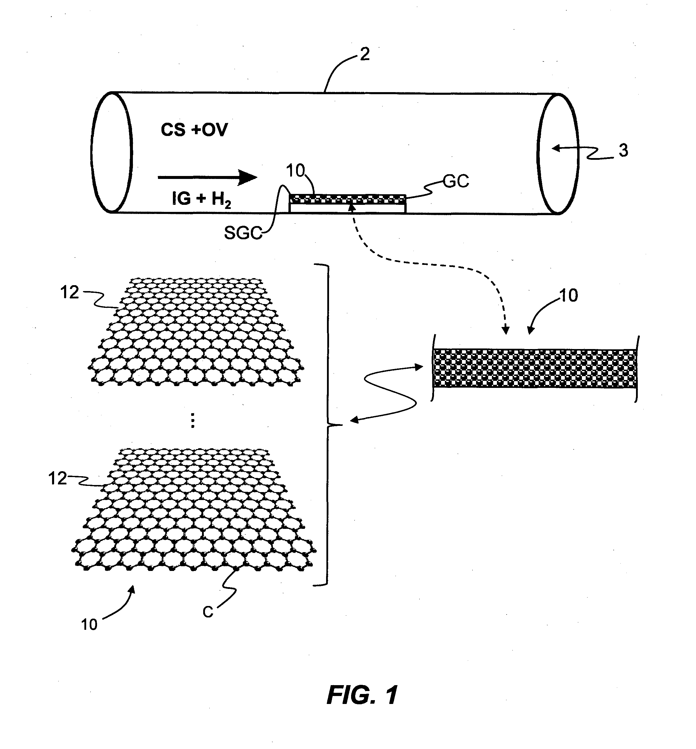
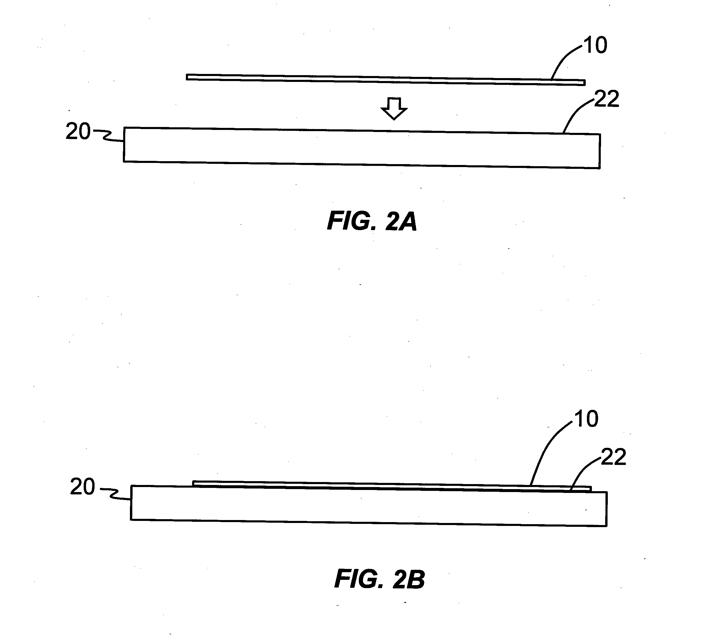
[0035]The multilayer graphene film may be formed according to the method illustrated in the schematic diagram of FIG. 1. FIGS. 2A and 2B illustrate an example of a graphene film 10 being placed on a surface 22 of a substrate 20, as described in greater detail below.

[0036]FIG. 1 shows a chemical-vapor-deposition (CVD) reaction chamber 2 that has an interior 3 that can be brought to a select high temperature and a select pressure to carry out the methods disclosed herein. In the disclosed methods, graphene film 10 is made up of one or more layers (sheets) of graphene 12, as shown in the close-up views, which shows the carbon atoms C in the characteristic hexagonal arrangement for graphene. The graphene film 10 is grown by CVD in CVD reaction chamber 2 using a gaseous carbon source CS and a weak oxidizing vapor (oxidizer) OV. The graphene film 10 made from multiple stacked individual sheets of graphene 12 can be formed by heat-treating gaseous carbon source CS in the presence of a grap...


PUM

PropertyMeasurementUnit
Temperatureaaaaaaaaaa
Timeaaaaaaaaaa

Abstract

Methods of growing a multilayer graphene film (10) include flowing a weak oxidizing vapor (OV) and a gaseous carbon source (CS) over a surface (SGC) of a carbonizing catalyst (GC) in a CVD reaction chamber (2). Carbon atoms (C) deposit on the carbonizing catalyst surface to form sheets of single-layer graphene (12) upon cooling. The method generates a substantially uniform stacking of graphene layers to form the multilayer graphene film. The multilayer graphene film is substantially uniform and has a relatively large scale as compared to graphene films formed by prior-art methods.

Description

FIELD[0001]This disclosure relates generally to methods of producing graphene and in particular to methods of growing substantially uniform, large-scale, multilayer graphene films.BACKGROUND ART[0002]Graphene is a one-atom-thick allotrope of carbon and has attracted attention due to its unique band structure and its structural, electrical and optical properties. Prototype devices incorporated with graphene, such as high-frequency field-effect transistors (FETs), photo-voltaic systems (solar cells), chemical sensors, super-capacitors, etc., have demonstrated the potential for the application of graphene in future electronics and opto-electronics devices. An overview of graphene is set forth in the article by A. K. Geim and K. S. Novoselov, entitled “The rise of graphene,”Nature Materials 6, no. 3 (2007): 183-191.[0003]To satisfy the widespread applications of graphene and the anticipated commercial demand for graphene-based products, it is critical to develop high-throughput and high...

Claims


Application Information

Patent Timeline
IPC IPC(8): C23C16/455C23C16/26C01B31/04C23C16/56
CPCC23C16/45517C01B31/0453C23C16/26C23C16/56B82Y40/00C01B2204/04C01B2204/32B82Y30/00C01B32/186
Inventor LOH, KIAN PINGZHANG, KAICASTRO NETO, ANTONIO HELIO
Owner NAT UNIV OF SINGAPORE
Why Eureka
Try Eureka