
Antenna device and communication terminal device

Active Publication Date: 2015-05-07
MURATA MFG CO LTD
View PDF4 Cites 2 Cited by
  • Summary
  • Abstract
  • Description
  • Claims
  • Application Information

AI Technical Summary

Benefits of technology

The present invention provides an antenna device that uses a conductor surface as a radiating element without slits or openings, overcoming issues of decreased mechanical strength, design restriction, and deteriorated field shield effect. The antenna coil is located in a way that prevents interference with other RF circuits, and a plurality of connecting conductors is used to improve its performance. Additionally, a capacitor can be used to further influence the carrier frequency, and the two conductor surfaces can be used as the radiating element to achieve certain antenna characteristics. Overall, the antenna device improves RF performance and provides more design flexibility.

Problems solved by technology

However, in the case where an enclosure of a terminal is “metallized”, there arises a problem in which communication with a counterpart antenna is prevented, because an electromagnetic field around an antenna incorporated in the terminal is shielded by a metal.
However, in a case where the metal plate is provided with a slit or an opening portion, consideration of decreased mechanical strength is required, and thus the number of man-hours required for production is increased.
In addition, particularly in a case where a metal enclosure is provided with a slit or an opening, there arises a restriction on enclosure design.
This causes a problem in which a field shield effect due to use of the metal plate is deteriorated, and a concern in which a first conductor surface and a second conductor surface might interfere with another radio frequency circuit.

Method used


Image

  • Antenna device and communication terminal device
  • Antenna device and communication terminal device
  • Antenna device and communication terminal device

Examples


first preferred embodiment

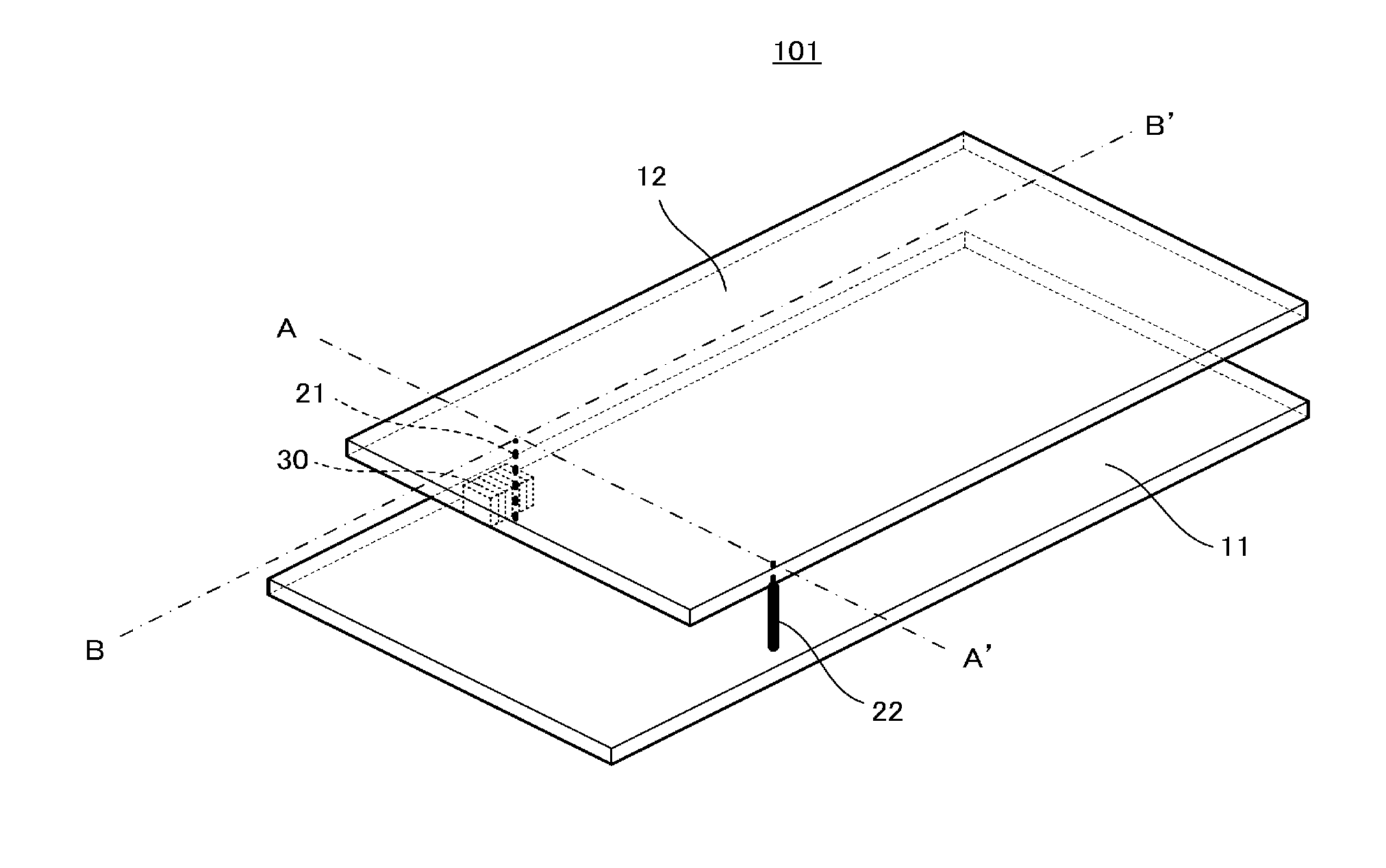
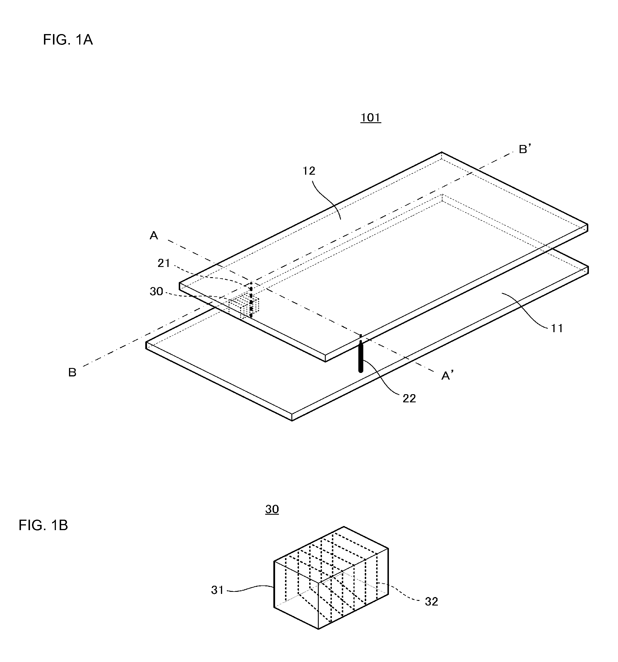
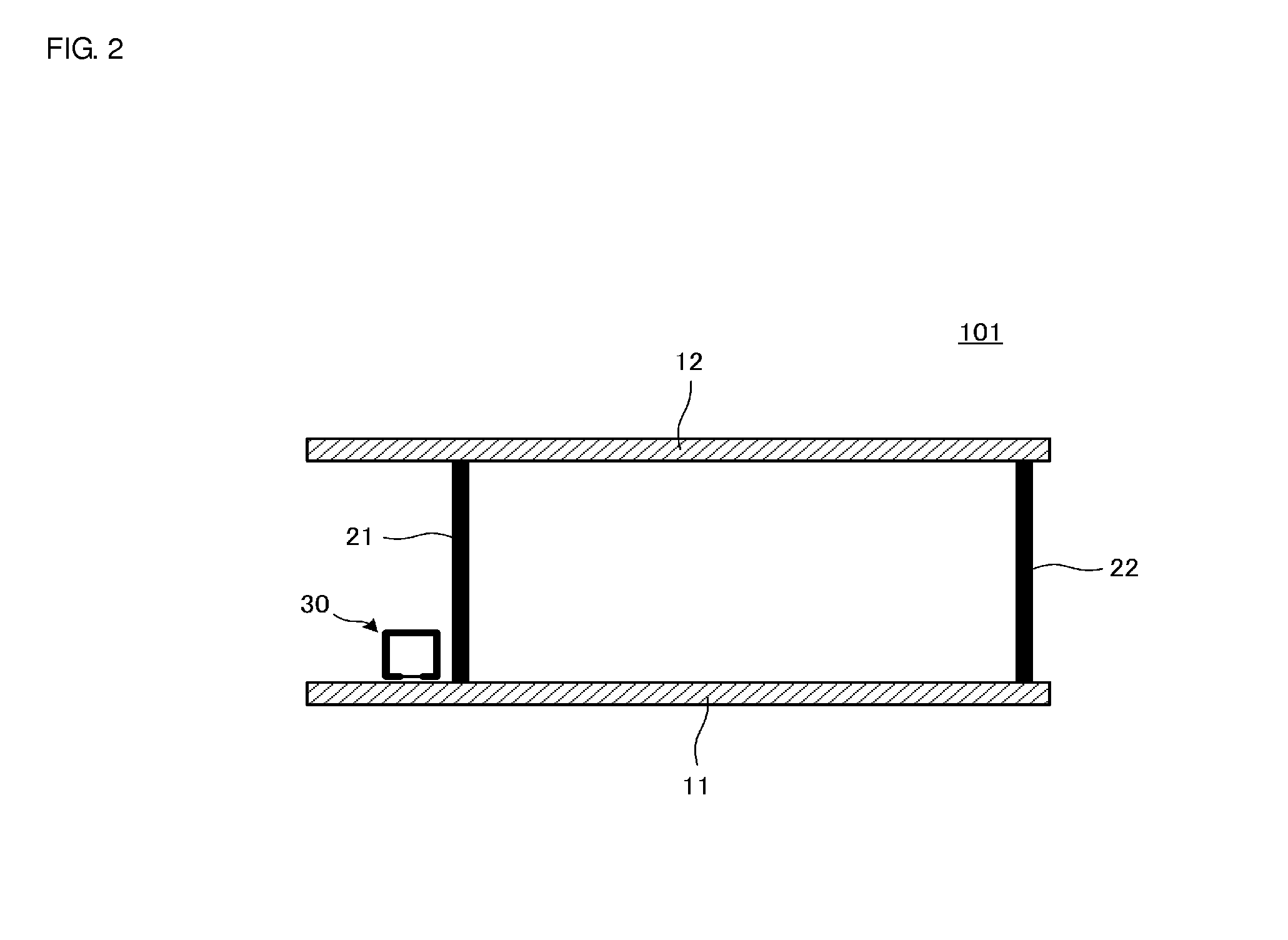
[0032]FIG. 1A is a perspective view of an antenna device 101 according to a first preferred embodiment of the present invention, and FIG. 1B is a perspective view of an antenna coil provided for the antenna device 101. FIG. 2 is a cross-sectional view taken along the line A-A′ in FIG. 1A. The antenna device 101 is preferably used for an HF band such as 13.56 MHz and is a proximity-type or vicinity-type antenna using electromagnetic (mainly magnetic) field coupling to a communication counterpart antenna, for example.

[0033]The antenna device 101 includes a first conductor surface 11 and a second conductor surface 12 that face each other and are spaced apart from each other. The first conductor surface 11 and the second conductor surface 12 are connected to each other through a first connecting conductor 21 and a second connecting conductor 22. The antenna coil 30 is located between the first conductor surface 11 and the second conductor surface 12 and in proximity to the first connect...

second preferred embodiment

[0044]FIG. 6 is a perspective view of an antenna device 102 according to a second preferred embodiment of the present invention. The antenna device 102 includes the first conductor surface 11 and the second conductor surface 12 that face each other. The first conductor surface 11 and the second conductor surface 12 are connected to each other through the first connecting conductor 21, the second connecting conductor 22, a third connecting conductor 23, and a fourth connecting conductor 24. The antenna coil 30 is located between the first conductor surface 11 and the second conductor surface 12 and in proximity to the first connecting conductor 21. In an example illustrated in FIG. 6, the connecting conductors 21 and 22 and the conductor surfaces 11 and 12 define a closed loop, the connecting conductors 21 and 23 and the conductor surfaces 11 and 12 define a closed loop, and the connecting conductors 21 and 24 and the conductor surfaces 11 and 12 define a closed loop. The antenna coi...

third preferred embodiment

[0046]FIG. 7A is a perspective view of a portion of a communication terminal device including an antenna device 103 according to a third preferred embodiment of the present invention. FIG. 7B is a perspective view of a portion of a communication terminal device including an antenna device in a comparative example. These communication terminal devices preferably are communication terminal devices each including an antenna 81 for the UHF band that is located in a circuit board. In the circuit board, a ground electrode that is the first conductor surface 11 is provided. In FIGS. 7A and 7B, the antenna 81 is an inverted-F antenna, but is schematically illustrated in the figures by using a conductor line. The antenna 81 for the UHF band is preferably used for calls and data communications by a mobile phone.

[0047]In the antenna device 103 in the present preferred embodiment illustrated in FIG. 7A, the first connecting conductor 21 is located inward of the edges of the first conductor surf...


PUM


Abstract

An antenna device includes two conductor surfaces facing each other and spaced apart from each other, connecting conductors that connect the two conductor surfaces at at least two positions, and an antenna coil located in proximity to one of the connecting conductors. The connecting conductors and the two conductor surfaces define a closed loop containing a surface of a space. In a plan view of the surface of the space defined by the closed loop, the antenna coil is located at a position where the antenna coil does not overlap the surface of the space and at a position where electromagnetic induction by the antenna coil causes an induced current to flow through the connecting conductor.

Description

BACKGROUND OF THE INVENTION[0001]1. Field of the Invention[0002]The present invention relates to an antenna device and a communication terminal device that are preferably used for a communication system for the HF band and the UHF band.[0003]2. Description of the Related Art[0004]Among devices provided for electronic devices such as mobile phones and that perform HF band communication such as near field communication (NFC), an RFIC and a matching element are generally mounted on a circuit board, and an antenna is attached to an inner surface of an enclosure of an electronic device. The RFIC and the antenna are electrically connected to each other through spring pins or the like.[0005]Meanwhile, wireless communication terminals such as recent mobile phones have been made increasingly thinner. To compensate for insufficient strength caused by such reduction in thickness, there are more cases than before where an enclosure is “metallized” such as a case where an enclosure is plated wit...

Claims


Application Information

Patent Timeline
IPC IPC(8): H01Q1/24H01Q7/00
CPCH01Q7/00H01Q1/243H01Q7/08H01Q9/0421H01Q9/42H01Q21/28
Inventor KATO, NOBORU
Owner MURATA MFG CO LTD
Learn More