Dual-metal gate CMOS devices and method for manufacturing the same

a technology of metal gate cmos and manufacturing method, which is applied in the field of semiconductor technology, can solve the problems of not being suitable for the threshold regulation of mos device, affecting the performance of mos device, and serious gate leakage, etc., and achieves the effect of simple process and convenient manufacturing

Inactive Publication Date: 2015-04-16
INST OF MICROELECTRONICS CHINESE ACAD OF SCI
View PDF3 Cites 31 Cited by
  • Summary
  • Abstract
  • Description
  • Claims
  • Application Information

AI Technical Summary

Benefits of technology

This patent describes a way to make semiconductor devices without causing damage to the underlying layers. The process involves depositing layers of metal with different properties in a specific order, and using a heat isolation layer to protect the first layer during a subsequent annealing process. This technique allows for the use of the first layer as a work function modulation layer for a second device, without the need for selective corrosion. Additionally, this method avoids negative impacts on the threshold modulation of other devices by avoiding the need to deposit a second layer of metal with the same properties as the first layer.

Problems solved by technology

Then, the ultra-thin conventional oxide or nitride oxide layer leads to a serious gate leakage.
Therefore, the traditional poly-Si / SiON system is no longer applicable.
However, poly-Si and high-K are combined to generate Fermi level pinning effect, which is not suitable for the threshold regulation of the MOS device.
Although this method is optimal, a variety of different metal gate materials and complex integration processes are required.
And the regulation scope is quite limited by employing a single metal post-process regulation method.
However, the above method still contains certain deficiencies:(1) Since different CMOS devices are corresponding to metal materials with different work functions, in the CMOS integration process, it is required to deposit the first type metal layer work function modulation layer in the entire device region and then perform selective corrosion to remove the first type metal layer work function modulation layer located in the second type device region.
However, selective corrosion is likely to cause damage to high-K materials on the surface of the second type device.
The addition of an etch stop layer may prevent damage to high-K materials, but may correspondingly result in increase of the process complexity and undermine the ability of the metal gate work function to modulate the device threshold.(2) The post-deposited second type metal layer deposition work function modulation layer, which is deposited simultaneously on the first type device, has some negative impacts on the threshold modulation of the first type device.

Method used


Image

  • Dual-metal gate CMOS devices and method for manufacturing the same
  • Dual-metal gate CMOS devices and method for manufacturing the same
  • Dual-metal gate CMOS devices and method for manufacturing the same

Examples


Embodiment Construction

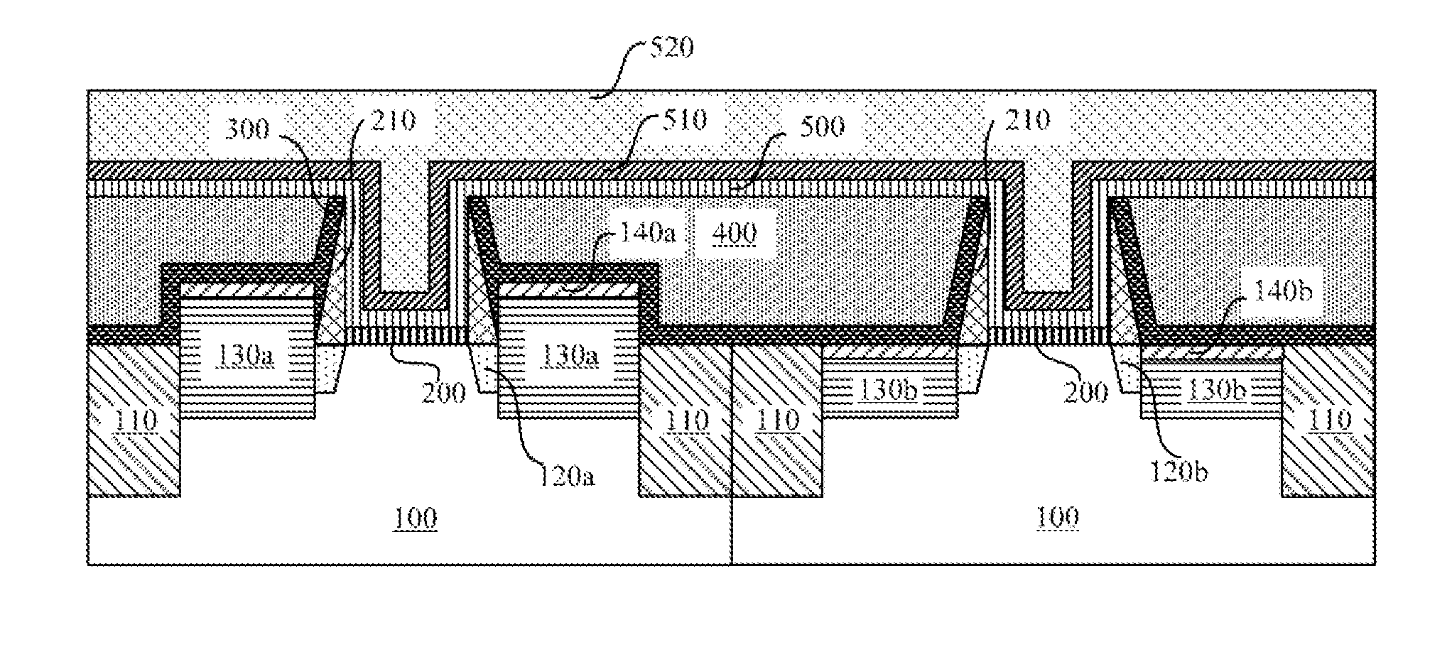
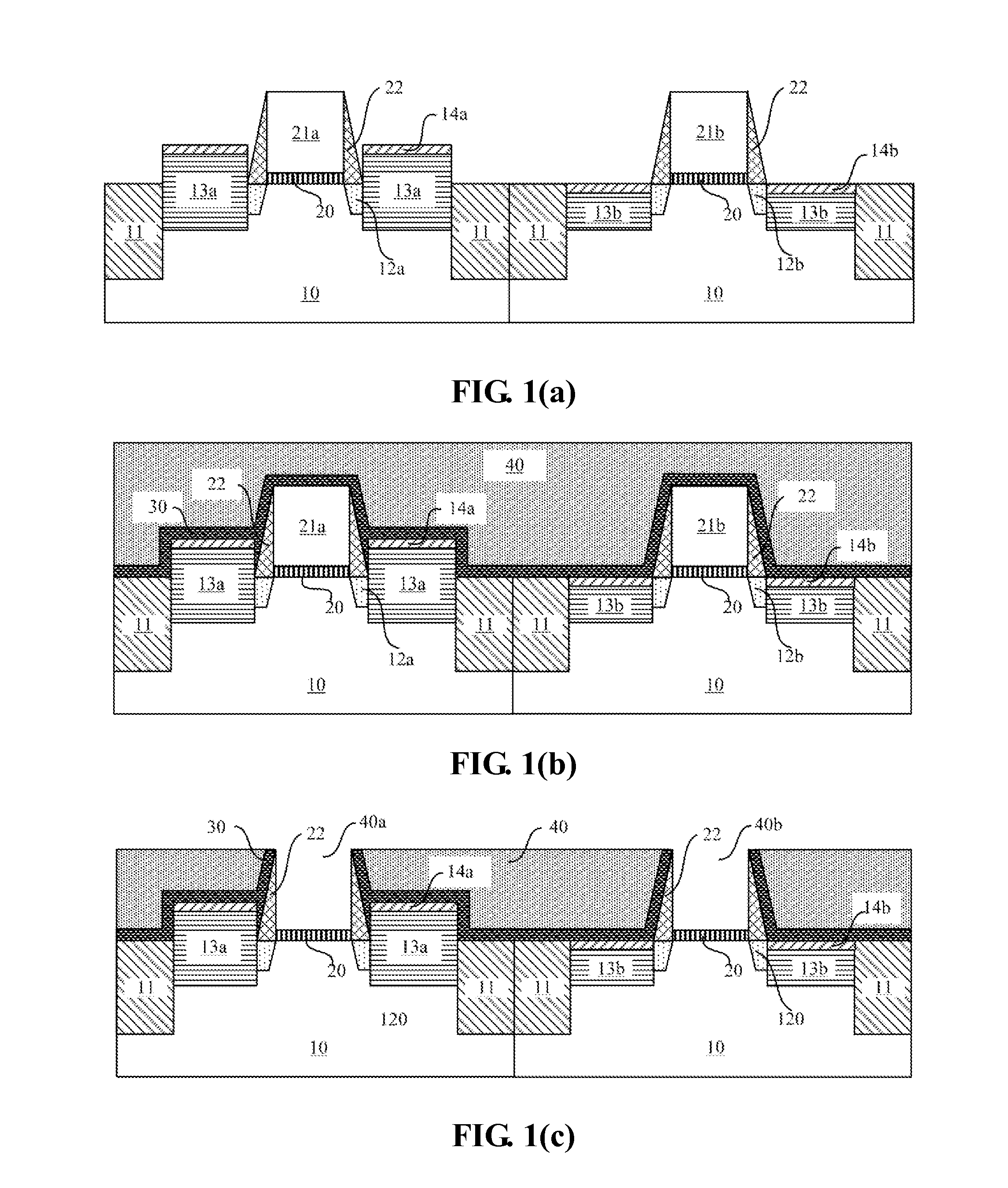
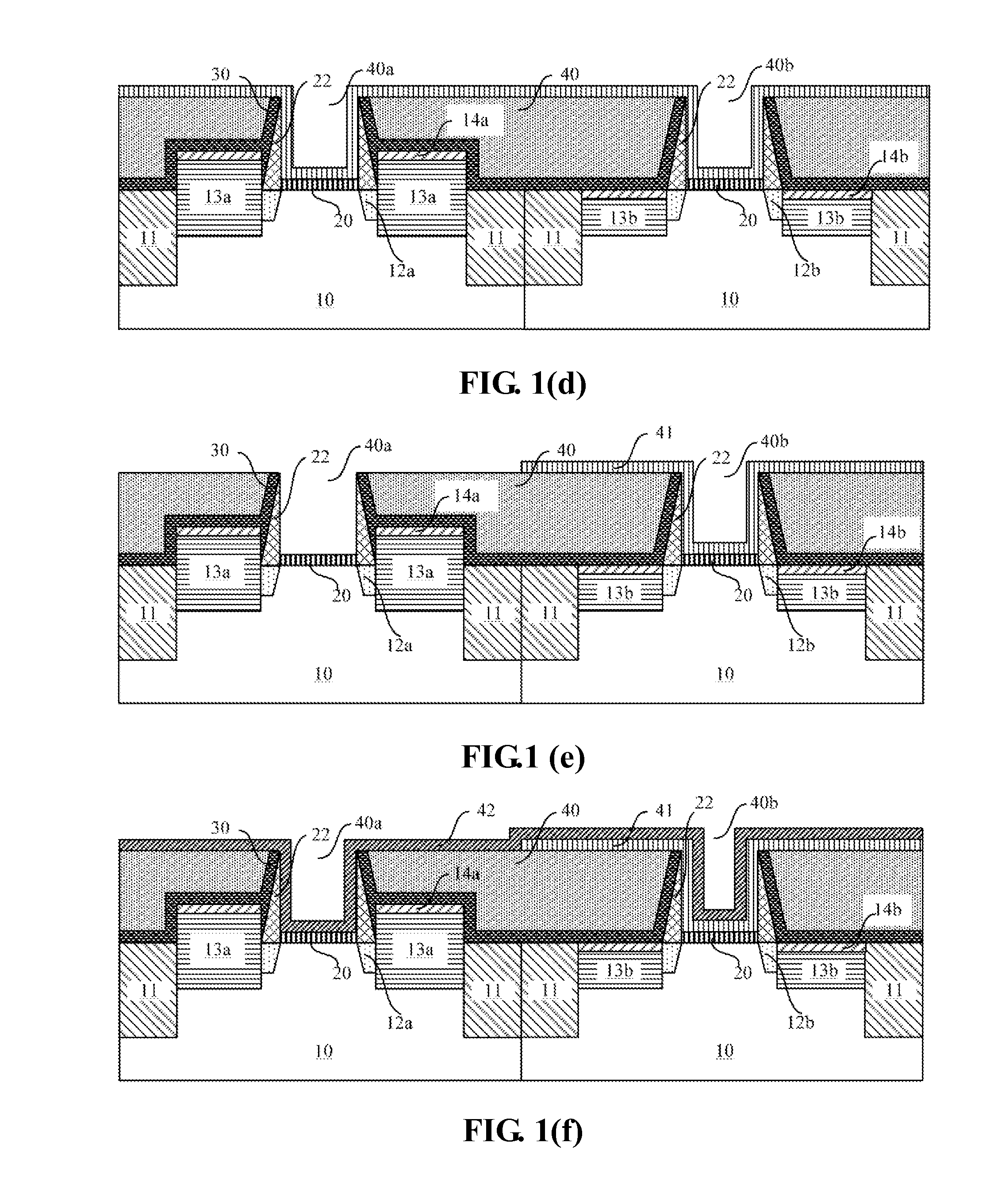
[0030]Exemplary embodiments of the present disclosure will be described in more details.

[0031]Some embodiments are illustrated in the attached drawings, in which the same or similar reference numbers represent the same or similar elements or the components having the same or similar functions. The following embodiments described with reference to the drawings are only exemplary for explaining the present invention, and therefore shall not be construed as limiting the present invention. The disclosure below provides many different embodiments or examples to implement different structures of the present invention. In order to simplify the disclosure of the present invention, components and settings of specific examples are described below. Obviously, they are merely exemplary, and are not intended to limit the present invention. In addition, reference numbers and / or letters can be repeated in different examples of the invention. This repetition is used only for brevity and clarity, an...


PUM

PropertyMeasurementUnit
work functionaaaaaaaaaa
equivalent oxide thicknessaaaaaaaaaa
thicknessaaaaaaaaaa

Abstract

A method for manufacturing a dual metal CMOS device comprising: forming a first type metal work function modulation layer in the first gate trench and the second gate trench; forming a second type work function metal diffusion source layer in the first gate trench and the second gate trench; forming a heat isolation layer that shields the region of the first type device; and thermally annealing the regions where the first type device and the second type device are located.

Description

CROSS REFERENCE TO RELATED APPLICATIONS[0001]This application claims the benefits of prior Chinese Patent Application No. 201210129587.7 filed on Apr. 27, 2012, titled “DUAL-METAL GATE CMOS DEVICES AND METHOD FOR MANUFACTURING THE SAME”, which is incorporated herein by reference in its entirety.TECHNICAL FIELD[0002]The present invention relates to a field of semiconductor technology. In particular, the present invention relates to a dual-metal gate CMOS device and a method for manufacturing the same.BACKGROUND OF THE ART[0003]Starting from the 45 nm CMOS IC process, as the feature size of the device increasingly shrinks, in order to suppress the short channel effect, the equivalent oxide thickness (EOT) of the gate dielectric layer must be reduced synchronously. Then, the ultra-thin conventional oxide or nitride oxide layer leads to a serious gate leakage. Therefore, the traditional poly-Si / SiON system is no longer applicable.[0004]The appearance of a high-K gate dielectric layer ef...

Claims


Application Information

Patent Timeline
Patent Type & Authority Applications(United States)
IPC IPC(8): H01L21/8234H01L29/51H01L27/092
CPCH01L21/82345H01L27/0928H01L29/517H01L21/823842H01L29/66545H01L27/092H01L29/66515H01L21/28H01L21/28008H01L21/28026H01L21/28044H01L21/28079H01L21/28088
Inventor YIN, HUAXIANGFU, ZUOZHENXU, QIUXIACHEN, DAPENG
Owner INST OF MICROELECTRONICS CHINESE ACAD OF SCI
Why Eureka
Try Eureka