Method for manufacturing thin-film solar modules, and thin-film solar modules which are obtainable according to this method

a technology of solar modules and solar cells, which is applied in the field of manufacturing photovoltaic thin-film solar modules and thin-film solar modules, can solve the problems of inability to exclude components, dopants, impurities, and contamination or interdiffusion of components, and achieves the effect of shortening the line distance, increasing the active surface area, and increasing the efficiency of thin-film solar modules

Inactive Publication Date: 2015-03-12
ROBERT BOSCH GMBH
View PDF2 Cites 7 Cited by
  • Summary
  • Abstract
  • Description
  • Claims
  • Application Information

AI Technical Summary

Benefits of technology

The present invention takes advantage of the use of a buffer layer in the manufacture of thin-film solar modules and provides a method for carrying out the first structuring step after application of the boundary layer(s) using laser treatment. This leads to improvements in efficiency and performance of the thin-film solar module. Additionally, the first and second structuring steps, as well as filling the structuring trench with insulating material, can be carried out in a single unit, leading to shorter line distances between the separating trenches and increased active surface area of individual solar cells. The use of very fine-dosing ink jet methods and quick-curing insulator ink or UV-curing, electrically insulating lacquer as filling material, along with the use of laser light pulses having a pulse duration of less than 10 picoseconds for the first and second laser treatments, allows for high-speed production.

Problems solved by technology

Due to plant engineering constraints, it is often extremely difficult or impossible to manufacture thin-film solar modules on a large scale having a module format with a size greater than 1.2 m×0.5 m. In addition, for the temperatures and reaction conditions to be used in the individual manufacturing stages, it has not been possible thus far to exclude contamination or interdiffusion of components, dopants, or impurities of individual layers of the multilayer system.

Method used


Image

  • Method for manufacturing thin-film solar modules, and thin-film solar modules which are obtainable according to this method
  • Method for manufacturing thin-film solar modules, and thin-film solar modules which are obtainable according to this method
  • Method for manufacturing thin-film solar modules, and thin-film solar modules which are obtainable according to this method

Examples


Embodiment Construction

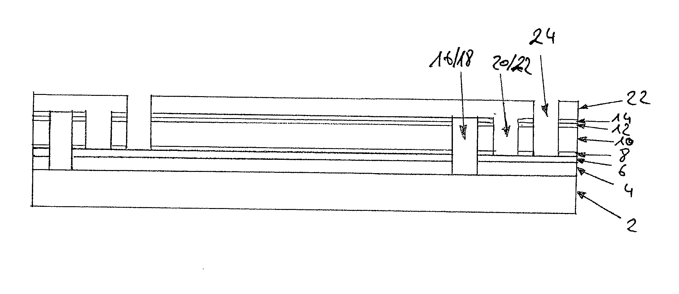
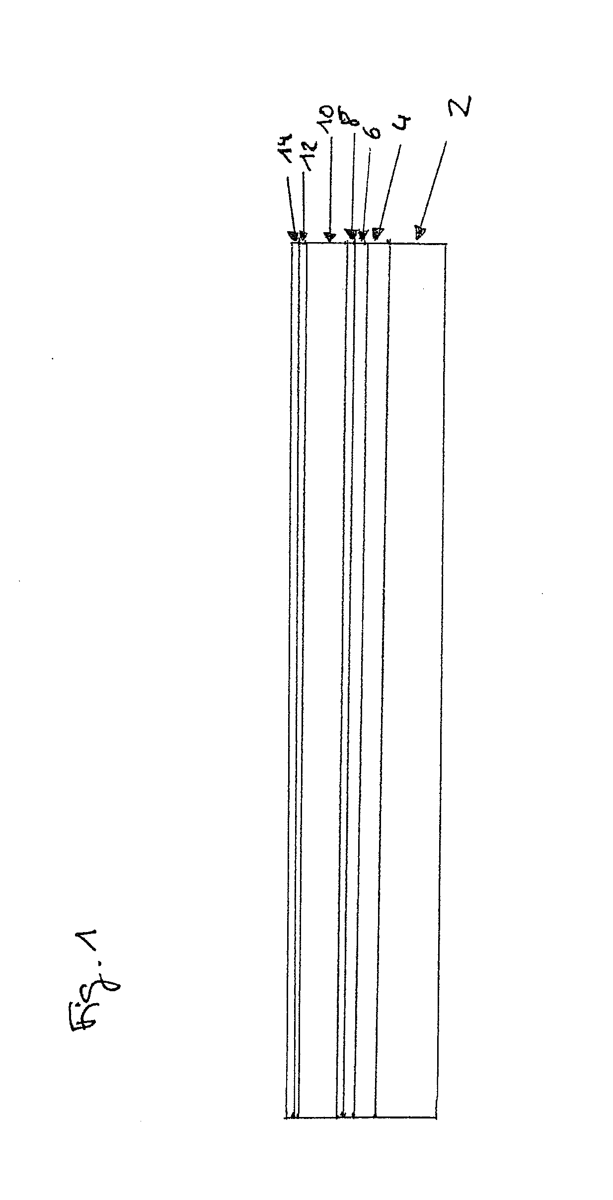
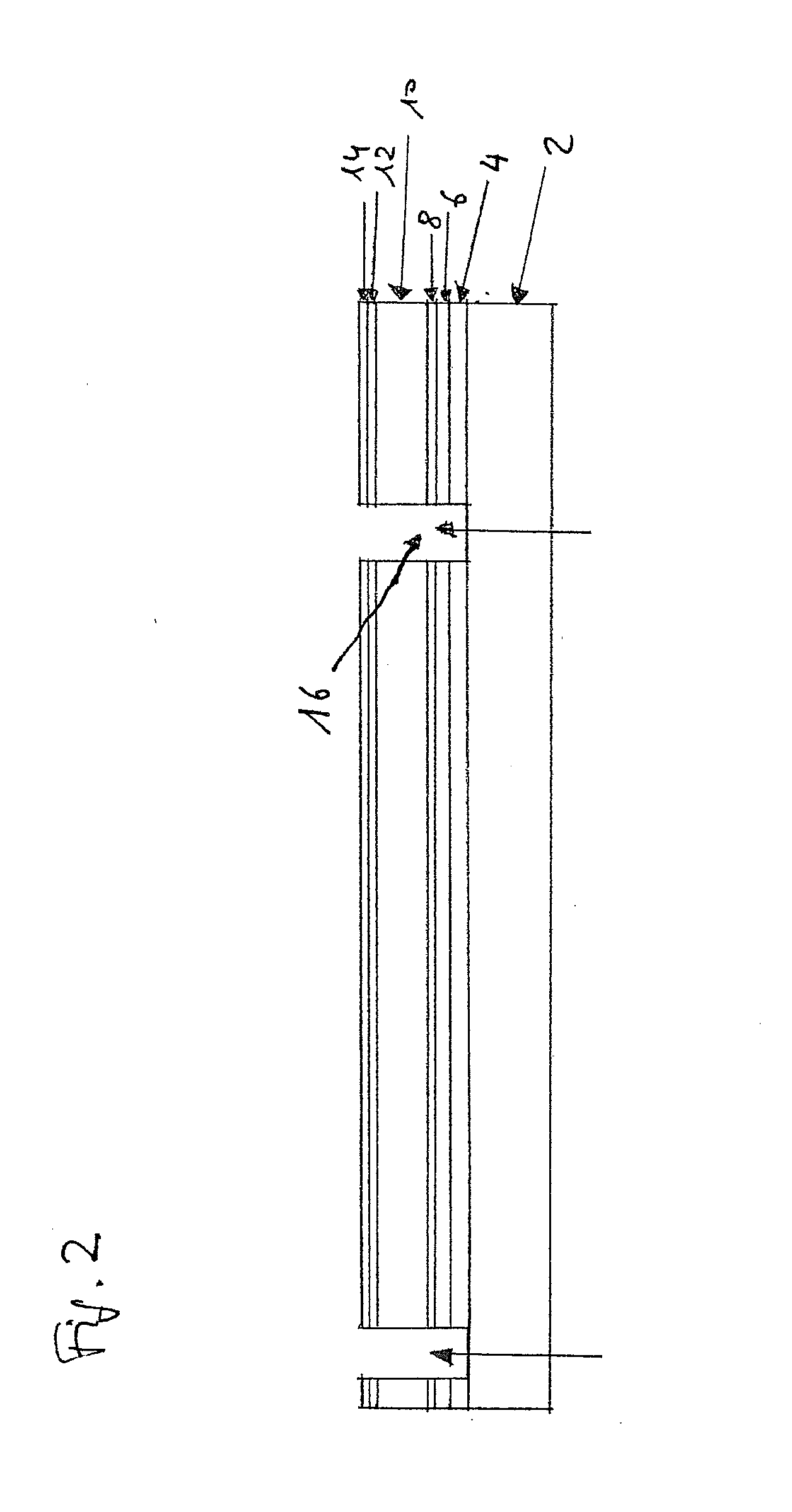
[0070]FIG. 1 shows a schematic cross-sectional view of an intermediate manufacturing stage 1a of a thin-film solar module 1 according to the present invention. A bulk back electrode layer 4 made of molybdenum and provided with the aid of thin-film deposition is present on glass substrate 2. The bulk back electrode layer is adjoined by a bidirectional reflective barrier layer 6 made of TiN or ZrN, for example, which likewise may be obtained with the aid of thin-film deposition. In the illustrated specific embodiment, an ohmic contact layer 8 made of a metal chalcogenide such as molybdenum selenide is situated on barrier layer 6. This contact layer may be obtained in various ways. In one embodiment, for example, molybdenum selenide from a molybdenum selenide target has been sputtered on. Alternatively, initially a metal layer may be applied which is subsequently converted into the corresponding metal chalcogenide before and / or during the formation of the semiconductor absorber layer. ...


PUM


Abstract

A method for manufacturing photovoltaic thin-film solar modules, including: applying a back electrode layer to a substrate, applying at least one conductive barrier layer, applying at least one contact layer, applying at least one kesterite or chalcopyrite semiconductor absorber layer, applying at least one buffer layer, removing the applied layers with laser treatment with formation of first separating trenches, filling the first separating trenches using at least one insulating material, removing layers extending from the barrier layer in the direction of the semiconductor absorber layer with formation of second separating trenches, or chemical phase transformation or thermal decomposition of layers extending from the barrier layer in the direction of the semiconductor absorber layer with the formation of first linear conductive areas, applying at least one transparent front electrode layer with filling and contacting of the second separating trenches or with contacting of the first linear conductive areas, so that adjacent solar cells are series connected, and removing the layers extending from the barrier layer in the direction of the front electrode layer with formation of third separating trenches. Described are such modules obtained by the method.

Description

FIELD OF THE INVENTION[0001]The present invention relates to a method for manufacturing photovoltaic thin-film solar modules, and the thin-film solar modules which are obtainable according to this method.BACKGROUND INFORMATION[0002]Photovoltaic thin-film solar modules are believed to have been understood and also commercially available. These types of modules may generally be based on the use of a so-called chalcopyrite semiconductor absorber layer, such as a Cu(In,Ga)(Se,S) system, and represent a complex multilayer system. The manufacture of such thin-film solar modules is a multistep process in which, due to numerous interactions, each method stage must be carefully coordinated with subsequent method stages. Due to plant engineering constraints, it is often extremely difficult or impossible to manufacture thin-film solar modules on a large scale having a module format with a size greater than 1.2 m×0.5 m. In addition, for the temperatures and reaction conditions to be used in the...

Claims


Application Information

Patent Timeline
Patent Type & Authority Applications(United States)
IPC IPC(8): H01L31/18H01L31/0224
CPCH01L31/186H01L31/022425H01L31/18H01L31/1884H01L31/0322H01L31/03923H01L31/0749Y02E10/541H01L31/0463Y02E10/52Y02P70/50
Inventor PROBST, VOLKER
Owner ROBERT BOSCH GMBH
Why Eureka
Try Eureka