
Wafer grounding and biasing method, apparatus, and application

Active Publication Date: 2015-02-19
ASML NETHERLANDS BV
View PDF1 Cites 4 Cited by
  • Summary
  • Abstract
  • Description
  • Claims
  • Application Information

AI Technical Summary

Benefits of technology

The invention provides an apparatus and method for grounding and biasing a wafer in a charged particle beam apparatus. The goal is to have a simple architecture and operation that allows for easy optimization of the grounding drive condition while minimizing damage to the wafer. The invention ensures a stable and low-resistance path for the bias current.

Problems solved by technology

Therefore, the required conductance between the contact(s) and the wafer substrate generally cannot be established by simply pressing the contact(s) against the wafer's backside surface.
The mechanical piercing method is simple and reliable, but it tends to create a large number of particles which may interfere with efforts to obtain high manufacturing yield of the finished products, i.e. semiconductor chips.
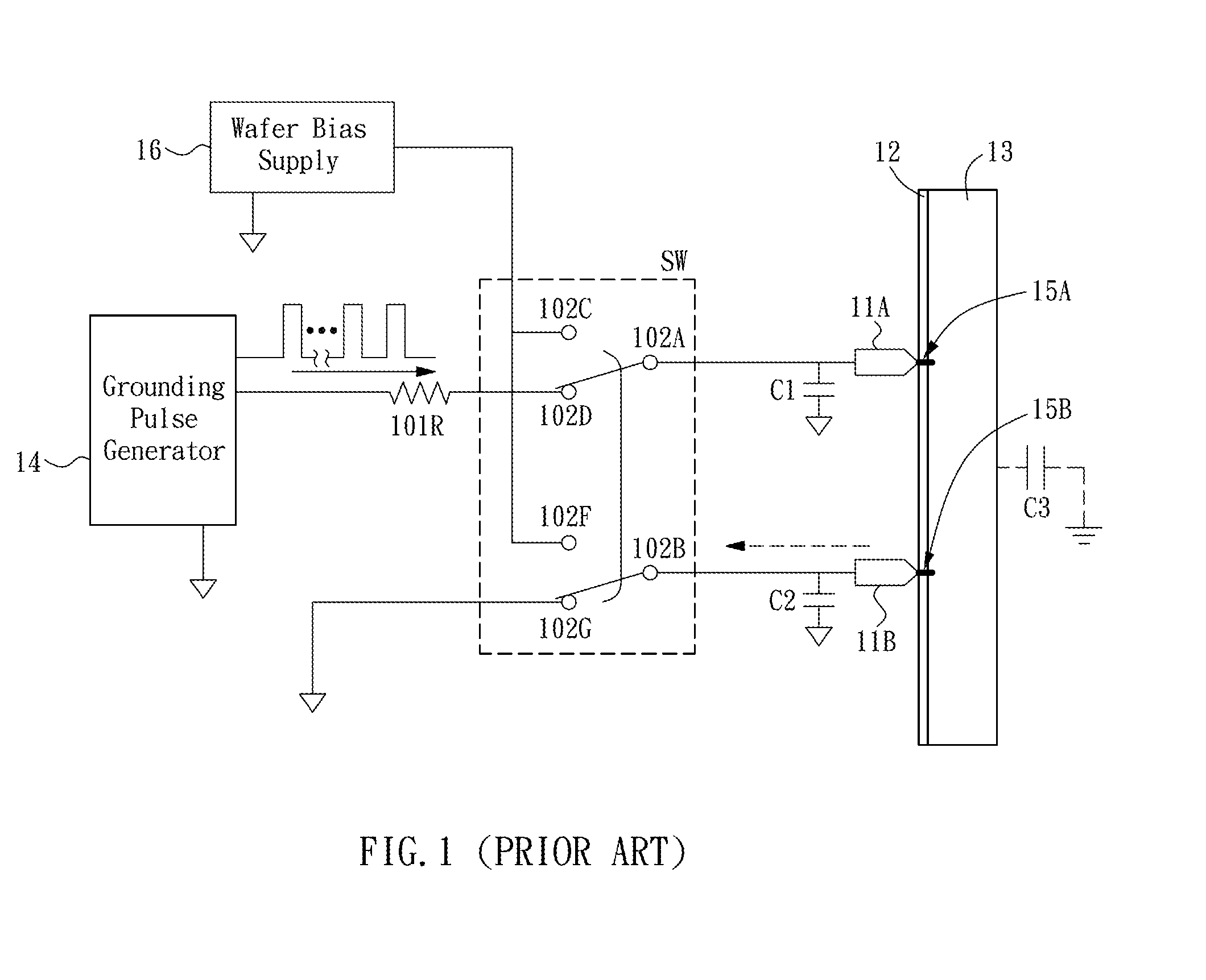
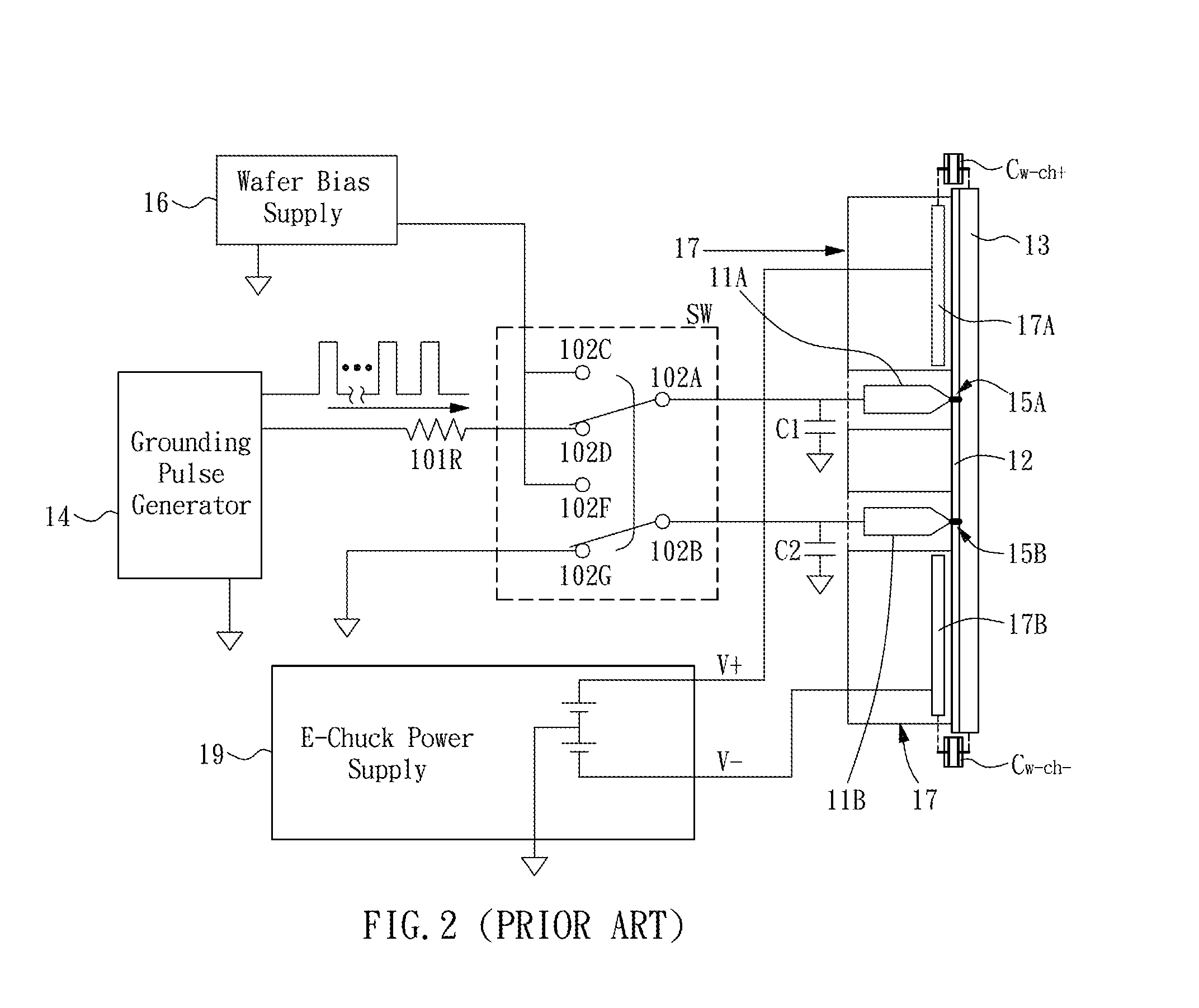
The grounding pulse current may also lead to further damages on the backside film(s) 12 as it continues.
Therefore, more severe structural damage on the backside film(s) in the vicinity of the neutralizing pin 11B may result.

Method used


Image

  • Wafer grounding and biasing method, apparatus, and
application
  • Wafer grounding and biasing method, apparatus, and
application
  • Wafer grounding and biasing method, apparatus, and
application

Examples


first embodiment

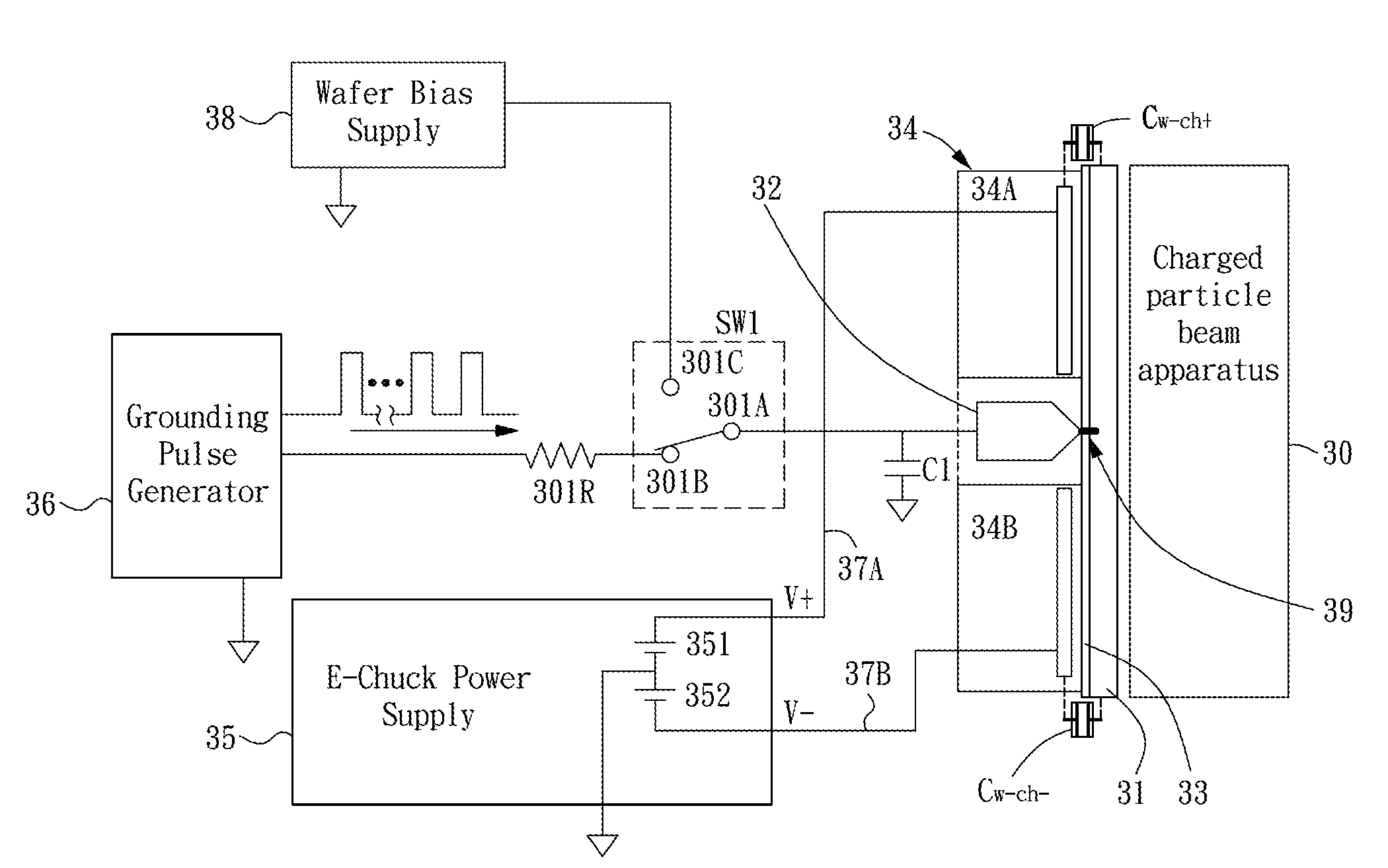
[0038]FIG. 3A is a schematic illustration of a wafer grounding and wafer biasing apparatus adaptable to a charged particle beam apparatus 30 according to the present invention. FIG. 3B illustrates a flow diagram associated with the apparatus of FIG. 3A. It is noted that in the following descriptions, same reference numerals are used to denote the same elements as in the previous embodiment (FIG. 1 and FIG. 2) where applicable.

[0039]Referring to FIG. 3A and FIG. 3B, before the wafer substrate 31 is subjected to the electron beam inspection, the wafer substrate 31 may be supported and held, in the step 395, by a wafer mount 34, which is capacitively coupled to the wafer substrate 31 according to the current embodiment. In this specification, “capacitively coupled” means that substantive capacitance is formed between the wafer substrate 31 and conductive element(s) of the wafer mount 34. The conductive element(s) must be electrically connected to the system ground (or its equivalent) t...

second embodiment

[0067]FIG. 5 is a schematic illustration of a wafer grounding and wafer biasing apparatus according to the present invention. Same reference numerals are used here to denote the same elements as in the previous embodiment (FIG. 3A) where applicable. In the embodiment, multiple (drive-end) pulse current pins 32 are used to acquire multiple wafer bias current paths. Only one of the pulse current pins 32 is driven to make the wafer bias current path at a time by the grounding pulse generator 36, while the rest of the pulse current pins 32 are kept floating or connected to an appropriate electrical node through high impedance path by using a switch array SW2 (which comprises multiple switches 501 that can be switched on / off), which selects one of the multiple pulse current pins 32 to be driven by the grounding pulse generator 36 at a time. By repeating the above grounding action (as described in conjunction with FIG. 3A) for the individual pin 32, multiple wafer bias current paths will ...


PUM


Abstract

A wafer grounding apparatus and method adaptable to a charged particle beam apparatus is disclosed. A wafer substrate is supported by a wafer mount. A pulse current pin is arranged to be in contact with a backside film formed on a backside of the wafer substrate. A grounding pulse generator provides at least one pulse to drive the pulse current pin such that dielectric breakdown occurring at the backside film leads to establishment of a current path through the backside films. Accordingly, a current flows in the wafer substrate through this current path and then flows out of the wafer substrate via at least one current return path formed from capacitive coupling between the wafer substrate and the wafer mount.

Description

CROSS REFERENCE TO RELATED PATENT APPLICATION[0001]This patent application is a continuation in part of U.S. patent application Ser. No. 12 / 552,270 filed Sep. 1, 2009, the contents of which are incorporated herein by reference.FIELD OF THE INVENTION[0002]The present invention generally relates to a charged particle beam apparatus, and more particularly to a wafer grounding and biasing apparatus and method thereof adaptable to a charged particle beam apparatus for semiconductor wafer manufacture.BACKGROUND OF THE INVENTION[0003]A charged particle beam apparatus is one which is able to produce a 2-dimensional image of a wafer substrate by detecting secondary electrons, backscattered electrons, mirror electrons, or other kind of electrons from the surface of the wafer substrate upon impingement by a charged particle beam generated by a charged particle beam apparatus, Various charged particle beam apparatus are used on semiconductor wafers in the semiconductor industry for various purp...

Claims


Application Information

Patent Timeline
IPC IPC(8): H01L21/683
CPCH01L21/6831B82Y10/00B82Y40/00H01J37/20H01J37/28H01J37/3174H01J2237/0044H01J2237/2008
Inventor WANG, YI-XIANGDOU, JUYINGKANAI, KENICHI
Owner ASML NETHERLANDS BV
Learn More