
Removing method

a technology of material layer and removal method, which is applied in the direction of basic electric elements, electrical equipment, semiconductor devices, etc., can solve the problems of difficult to obtain a vertical structure through wet etching, small gaps between patterns, and by-products generated by wet etching process are easy to remain in small gaps, so as to reduce the loading effect and effectively remove the material layer

Active Publication Date: 2015-02-12
UNITED MICROELECTRONICS CORP
View PDF1 Cites 21 Cited by
  • Summary
  • Abstract
  • Description
  • Claims
  • Application Information

AI Technical Summary

Benefits of technology

The invention provides a way to effectively remove a layer of material while reducing the impact on the underlying structure. This is done by performing a cycle process multiple times.

Problems solved by technology

However, it is difficult to obtain a vertical structure through the wet etching.
However, with the continued miniaturization of a device size, by-products generated by the dry etching process are easy to remain in small gaps between patterns.
Therefore, the undesired thickness of the material layer below the gaps can not be etched completely, and the serious loading effect and other issues occur.

Method used


Image

  • Removing method
  • Removing method
  • Removing method

Examples


Embodiment Construction

[0034]Reference will now be made in detail to the present preferred embodiments of the invention, examples of which are illustrated in the accompanying drawings. Wherever possible, the same reference numbers are used in the drawings and the description to refer to the same or like parts.

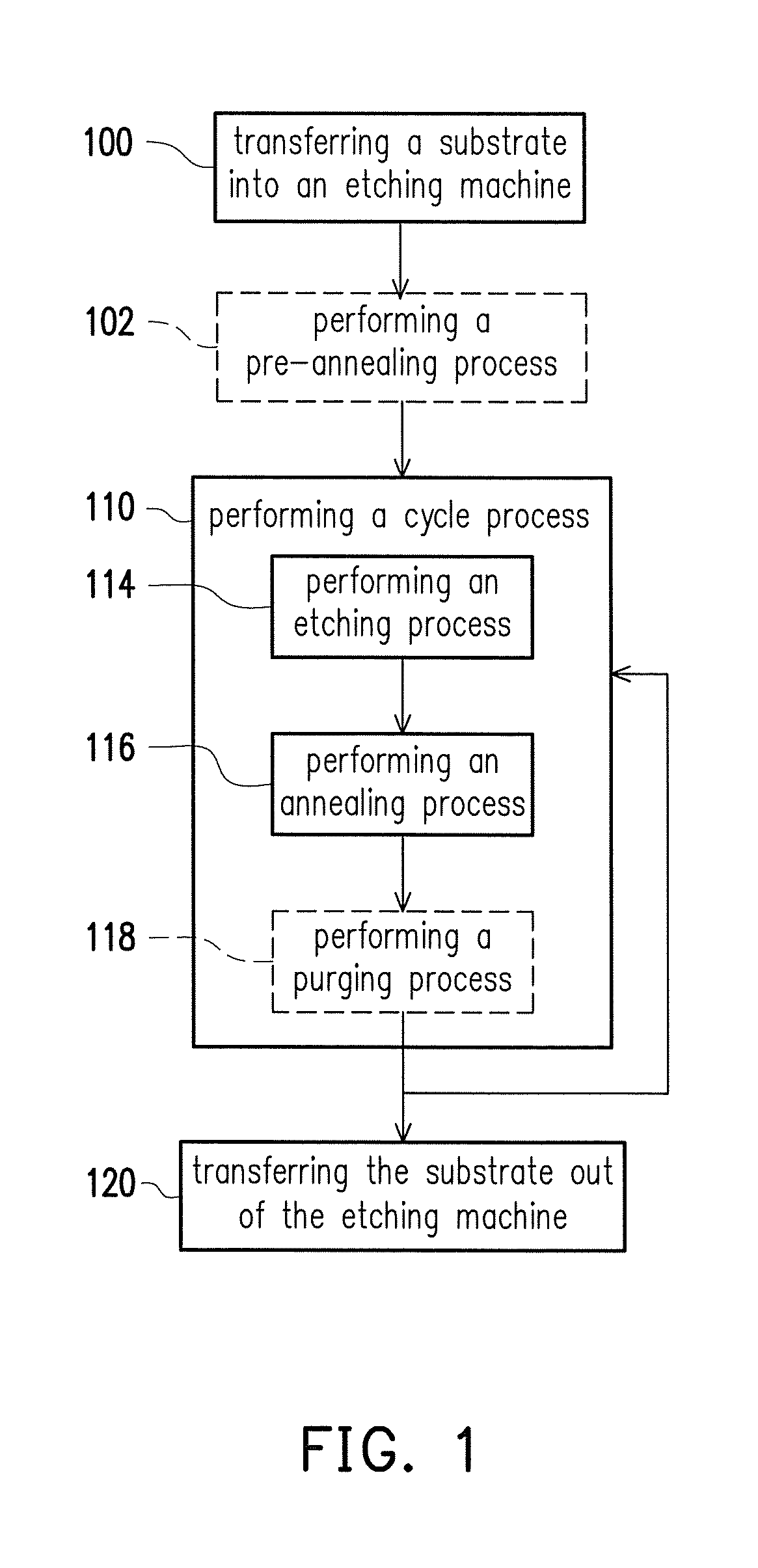
[0035]In the removing process of the invention, a material layer is removed by repeating a cycle process including an etching and an annealing at least one time, and optionally by performing a pre-annealing prior to the cycle process. The cycle process can be performed multiple times to effectively remove the material layer and reduce the loading effect. The embodiments of the invention are described in detail below, but the invention is not limited thereto.

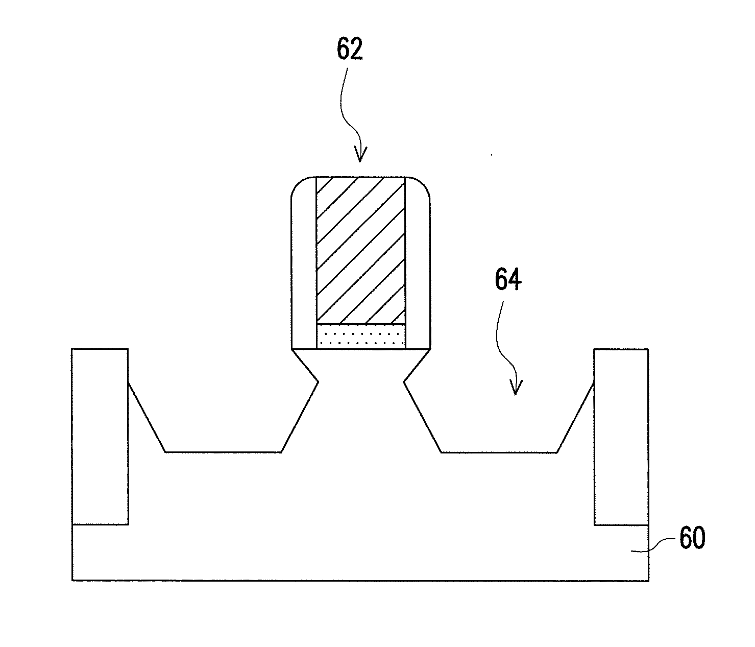
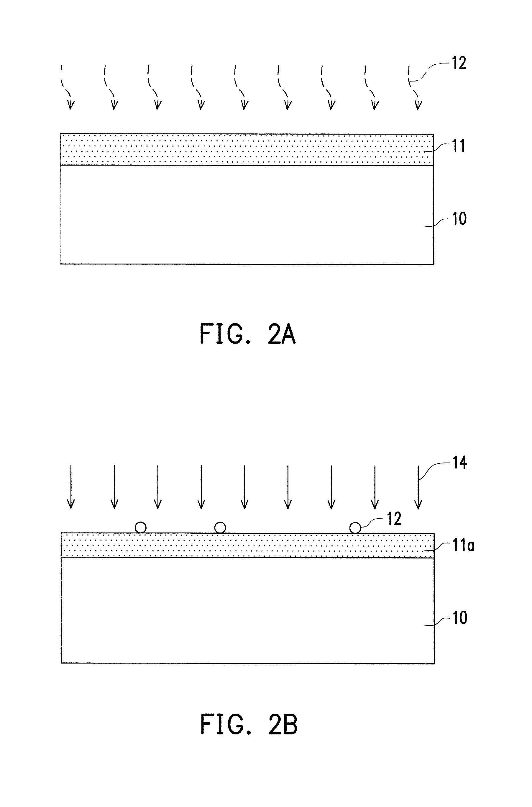
[0036]FIG. 1 illustrates a process flow of a removing process according to an embodiment of the present invention. FIG. 2A to FIG. 2E illustrate schematic cross-sectional views of a removing process according to an embodiment of the present invent...


PUM


Abstract

A removing method including the following steps. A substrate is transferred into an etching machine, wherein the substrate has a material layer formed thereon. A cycle process is performed. The cycle process includes performing an etching process to remove a portion of the material layer, and performing an annealing process to remove a by-product generated by the etching process. The cycle process is repeated at least one time. The substrate is transferred out of the etching machine. In the removing method of the invention, the cycle process is performed multiple times to effectively remove the undesired thickness of the material layer and reduce the loading effect.

Description

BACKGROUND OF THE INVENTION[0001]1. Field of Invention[0002]The present invention relates to an integrated circuit process, and more particularly to a removing process.[0003]2. Description of Related Art[0004]An etching process is a commonly used method to remove a film layer in a semiconductor process. The etching process generally includes a wet etching and a dry etching. The wet etching provides a higher etching selectivity and is suitable for an isotropic etching process. However, it is difficult to obtain a vertical structure through the wet etching. When more and more devices are developed toward high aspect ratio structures, the dry etching is adopted due to its excellent performance. Besides, the dry etching has the advantages of better control of etching rate, precise etched dimension and high degree of automation etc.[0005]However, with the continued miniaturization of a device size, by-products generated by the dry etching process are easy to remain in small gaps between ...

Claims


Application Information

Patent Timeline
Patent Type & Authority Applications(United States)
IPC IPC(8): H01L21/311
CPCH01L21/31116H01L21/02057H01L21/02046H01L29/66636H01L29/7848H01L29/66795H01L21/76224
Inventor LIAO, CHIN-ITUNG, YU-CHENG
Owner UNITED MICROELECTRONICS CORP
Learn More