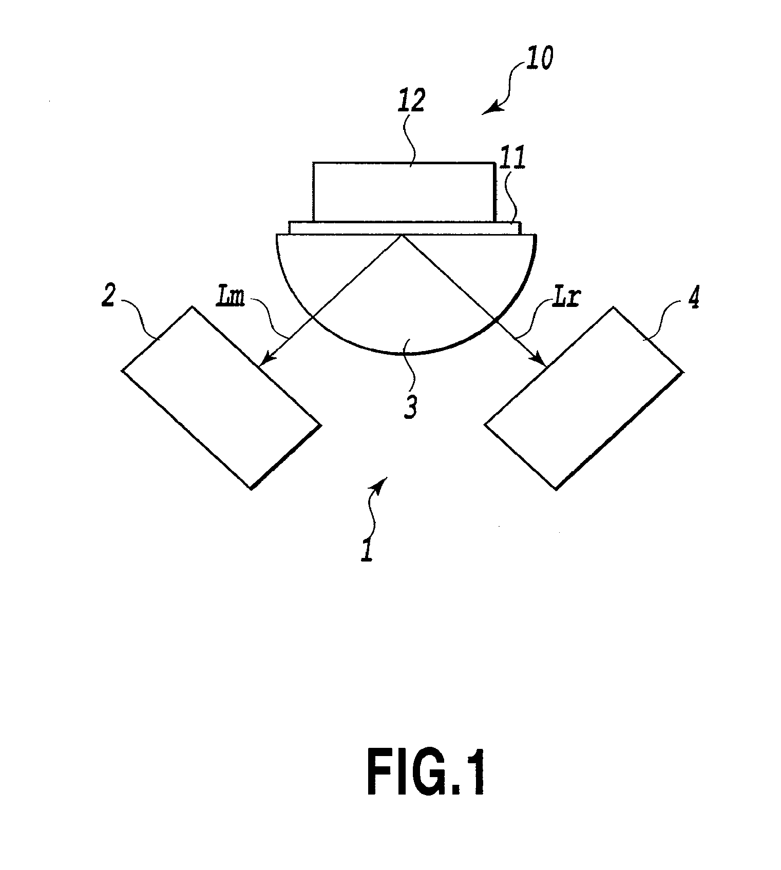
Chip for optical analysis
a technology of optical analysis and chips, applied in the field of chips for optical analysis, can solve the problems of inability to perform pretreatment operations, inability to eliminate impurities, inability to perform simple measurement, etc., and achieve the effect of accurate liquid analysis, low cost and high sensitivity
- Summary
- Abstract
- Description
- Claims
- Application Information
AI Technical Summary
Benefits of technology
Problems solved by technology
Method used
Image

Examples
example 1
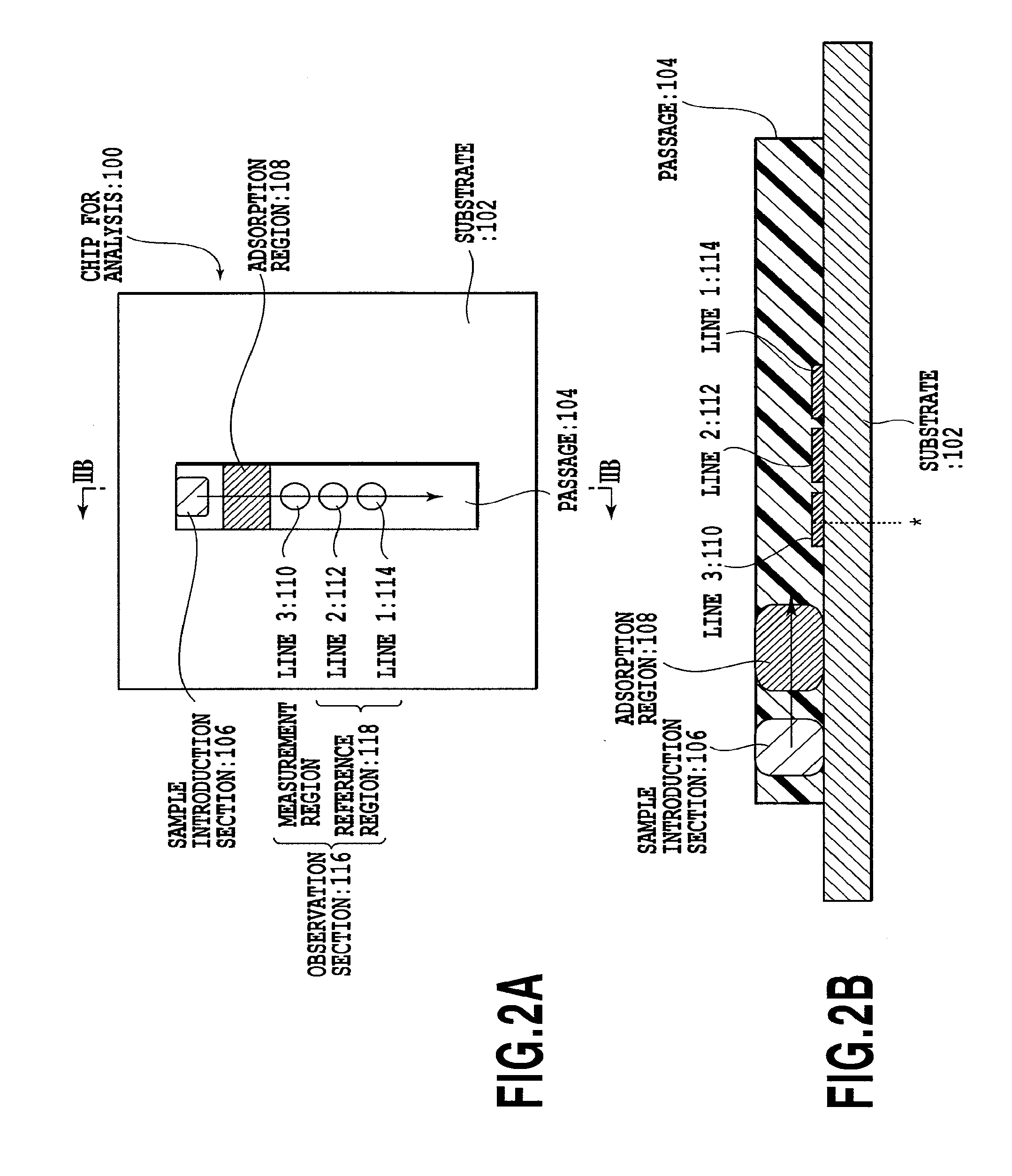
[0154]This example shows a chip for optical analysis for a passage without a bypass passage as shown in FIGS. 2A and 2B, for which a protein A adsorbent is used as an adsorbent.
[0155]Cellulose acetate was dissolved in an organic solvent to prepare a cellulose acetate solution. A gold thin film (thickness 50 nm) was formed on a BK7 glass substrate by vapor-deposition. A resist membrane or a tape was applied onto this gold thin film, and a pattern in which a portion of the gold thin film corresponding to a passage was exposed was formed. The patterned gold / glass substrate was mounted on a spin coater, the cellulose acetate solution prepared beforehand was added dropwise to the substrate, then the substrate was rotated, and the organic solvent was evaporated to form a white membrane-form passage. Subsequently, a buffer solution of protein A was prepared and added dropwise to an adsorption region of the passage, and protein A was adsorbed to the passage to form the adsorption region. Th...
example 2
[0161]This example shows a chip for optical analysis for a passage without a bypass passage as shown in FIGS. 2A and 2B, for which a modified dextran microparticle adsorbent is used as an adsorbent.
[0162]A cellulose acetate solution obtained by dissolving cellulose acetate in an organic solvent and modified dextran microparticles (obtained from the microparticlation of methacrylate-modified dextran by radical polymerization) (diameter 15 to 30 μm) were mixed to prepare a cellulose acetate-dextran microparticle mixture solution. A gold thin film (thickness 50 nm) was formed on a BK7 glass substrate by vapor-deposition. A resist membrane or a tape was applied onto this gold thin film to form a pattern in which a portion of the gold thin film corresponding to a passage was exposed. At this time, an adsorption region of the passage on the metal thin film was prevented from being exposed, and the cellulose acetate solution was prevented from being deposited on the adsorption region. Subs...
example 3
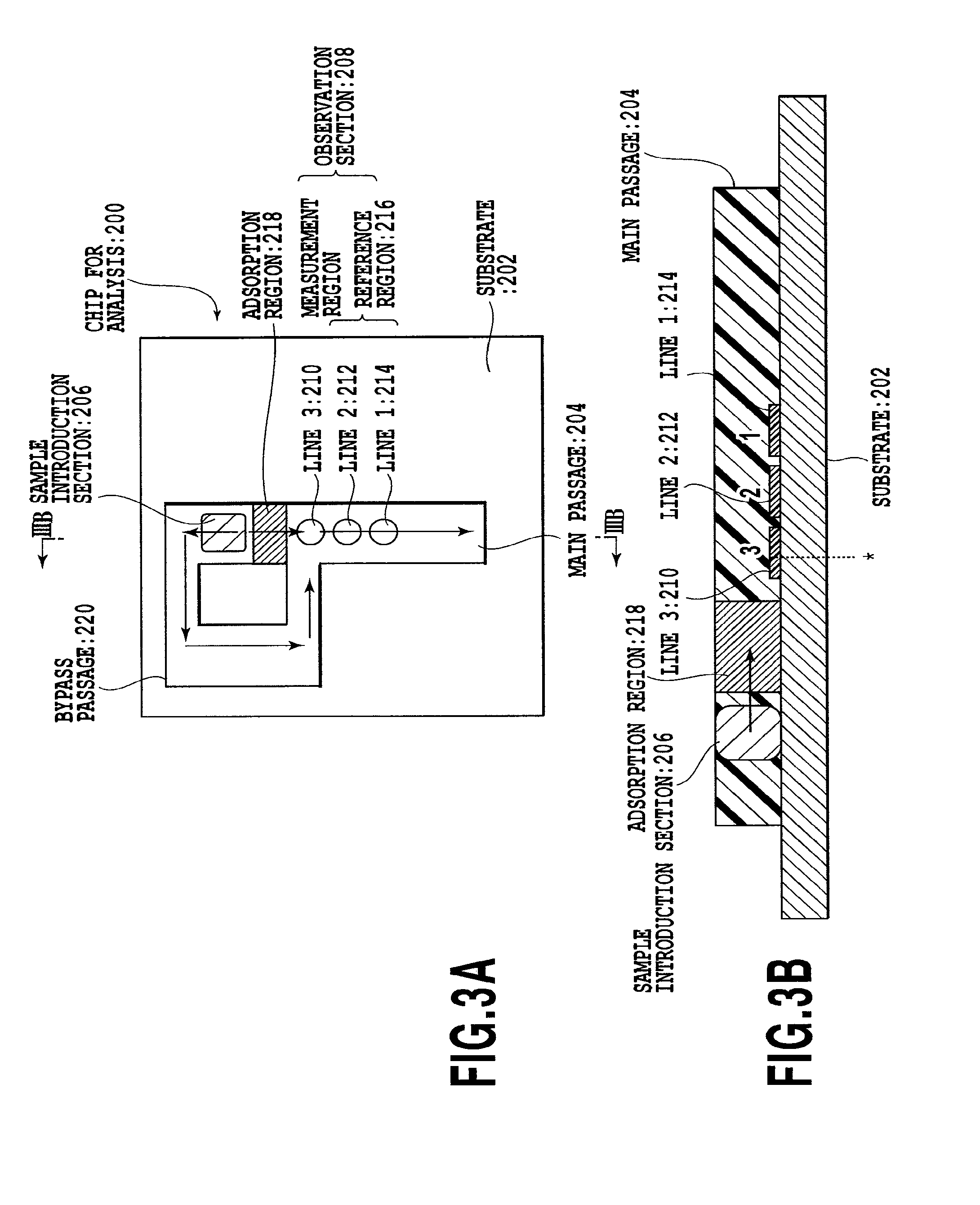
[0168]This example is a chip for optical analysis with a passage having a bypass passage as shown in FIGS. 3A and 3B using a protein A adsorbent as an adsorbent.
[0169]Cellulose acetate was dissolved in an organic solvent to prepare a cellulose acetate solution. A gold thin film (thickness 50 nm) was formed on a BK7 glass substrate by vapor-deposition. A resist membrane or a tape was applied onto this gold thin film, and a pattern in which portions of the gold thin film corresponding to the main passage and the bypass passage were exposed was formed. The patterned gold / glass substrate was mounted on a spin coater, the previously prepared cellulose acetate solution was added dropwise, then the substrate was rotated, and the organic solvent was evaporated to form white membrane-form main passage and bypass passage. Subsequently, a buffer solution of protein A was prepared and added dropwise onto an adsorption region of the passage, and protein A was adsorbed to the passage to form the ...
PUM
 Abstract
Description
Claims
Application Information
 - R&D
- Intellectual Property
- Life Sciences
- Materials
- Tech Scout
- Unparalleled Data Quality
- Higher Quality Content
- 60% Fewer Hallucinations
Browse by: Latest US Patents, China's latest patents, Technical Efficacy Thesaurus, Application Domain, Technology Topic, Popular Technical Reports.
© 2025 PatSnap. All rights reserved.Legal|Privacy policy|Modern Slavery Act Transparency Statement|Sitemap|About US| Contact US: help@patsnap.com