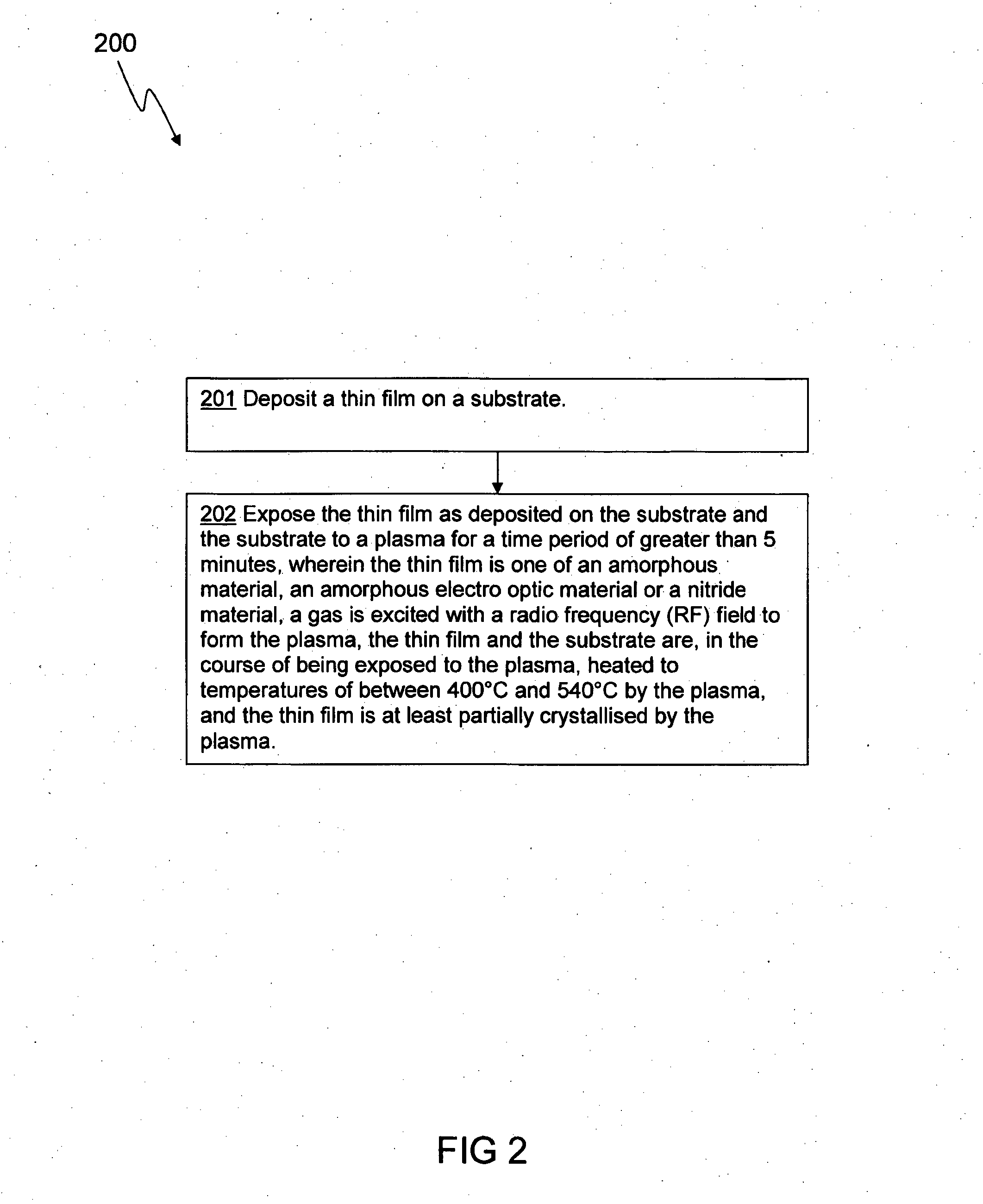
Methods of crystallising thin films
a technology of crystallization and thin films, applied in vacuum evaporation coatings, sputtering coatings, coatings, etc., can solve the problems of not being able to produce active magneto optics or active electro optic films on the same substrate as the integrated circuit, and requiring even higher thermal budgets. , to achieve the effect of reducing pressure, not oxidizing, and high conductivity
- Summary
- Abstract
- Description
- Claims
- Application Information
AI Technical Summary
Benefits of technology
Problems solved by technology
Method used
Image

Examples
Embodiment Construction
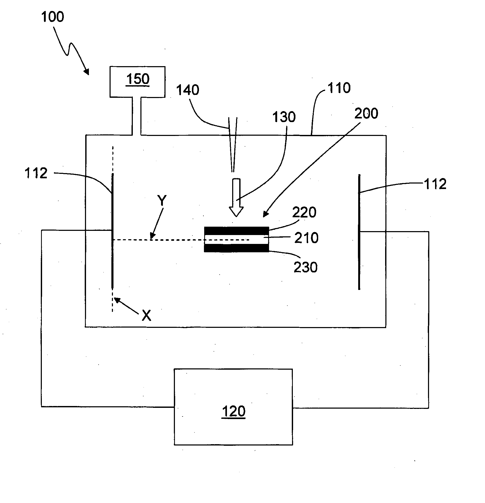
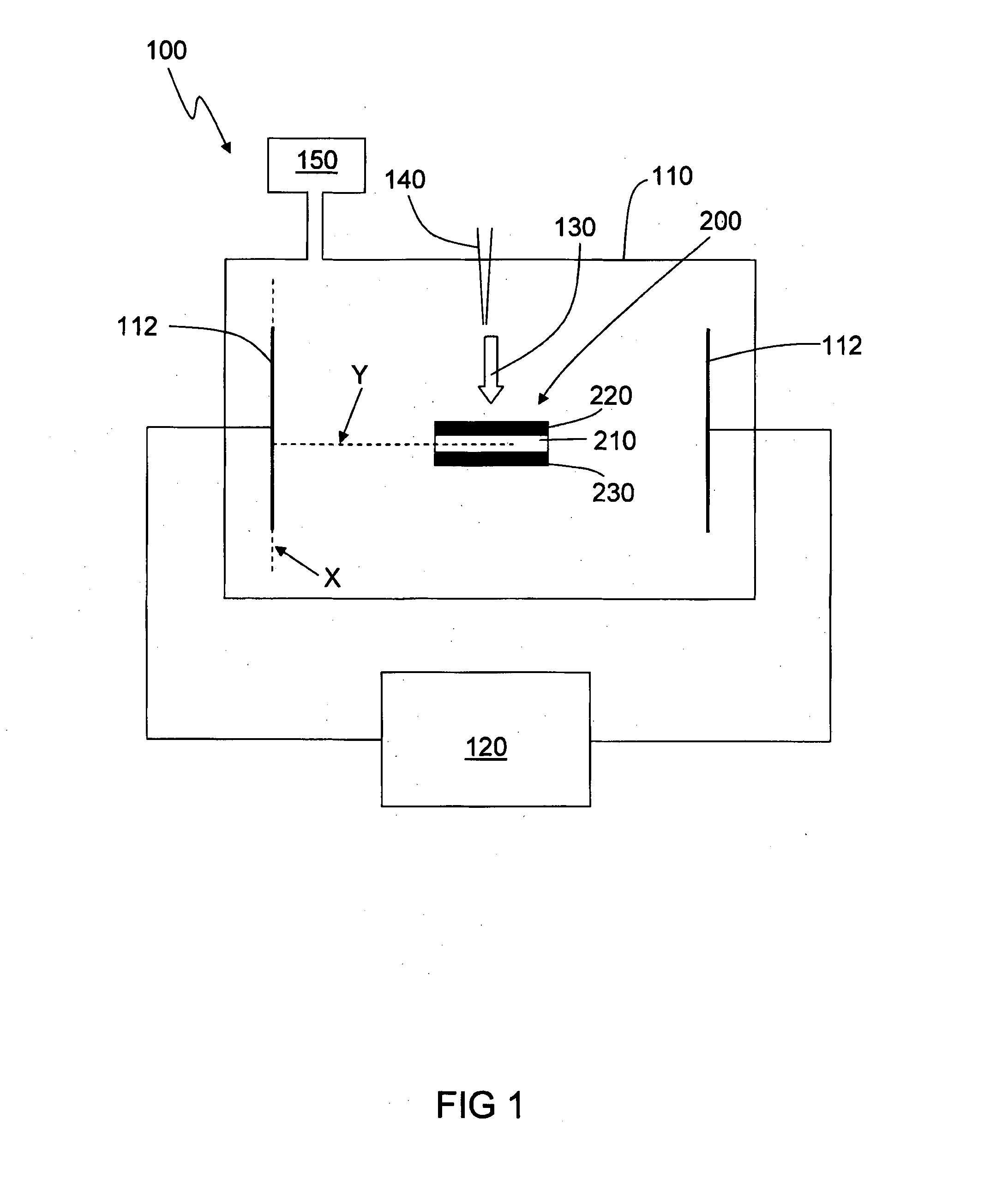
[0064]Elements of the invention are illustrated in concise outline form in the drawings, showing only those specific details that are necessary to understanding the embodiments of the present invention, but so as not to clutter the disclosure with excessive detail that will be obvious to those of ordinary skill in the art in light of the present description.
[0065]In this patent specification, adjectives such as first and second, left and right, front and back, top and bottom, etc., are used solely to define one element from another element without necessarily requiring a specific relative position or sequence that is described by the adjectives. Words such as “comprises” or “includes” are not used to define an exclusive set of elements or method steps. Rather, such words merely define a minimum set of elements or method steps included in a particular embodiment of the present invention. It will be appreciated that the invention may be implemented in a variety of ways, and that this ...
PUM
| Property | Measurement | Unit |
|---|---|---|
| temperatures | aaaaa | aaaaa |
| temperatures | aaaaa | aaaaa |
| pressure | aaaaa | aaaaa |
Abstract
Description
Claims
Application Information
 - R&D
- Intellectual Property
- Life Sciences
- Materials
- Tech Scout
- Unparalleled Data Quality
- Higher Quality Content
- 60% Fewer Hallucinations
Browse by: Latest US Patents, China's latest patents, Technical Efficacy Thesaurus, Application Domain, Technology Topic, Popular Technical Reports.
© 2025 PatSnap. All rights reserved.Legal|Privacy policy|Modern Slavery Act Transparency Statement|Sitemap|About US| Contact US: help@patsnap.com