
Method for fabricating defect free silicon mold insert

a technology of defect-free silicon and mold inserts, applied in the field of method for fabricating defect-free silicon mold inserts, can solve the problems of sapphire substrate defect, scratches and grid lines are the most common defects, penetrate the epitaxial wafer, and serious epitaxial defects, so as to increase the throughput of epitaxial wafer production

Inactive Publication Date: 2014-12-04
NANOCRYSTAL ASIA +1
View PDF1 Cites 5 Cited by
  • Summary
  • Abstract
  • Description
  • Claims
  • Application Information

AI Technical Summary

Benefits of technology

The present invention is about a method for making a defect-free silicon mold insert which can improve the production of epitaxial wafers. The method involves creating a pattern on the silicon mold insert, coating it with metal, and then removing the pattern to form the final mold insert. This process can create a uniform pattern and eliminate grid lines on the epitaxial wafers, leading to higher production efficiency. The defect-free silicon mold insert produced by this method is easy to apply, cost-effective, and reproducible, making it a good replacement for the current expensive and defect-prone methods used for producing nano imprint molds. Overall, the present invention has the technical effects of creating a uniform pattern and ensuring equal distance between patterns on the silicon mold insert.

Problems solved by technology

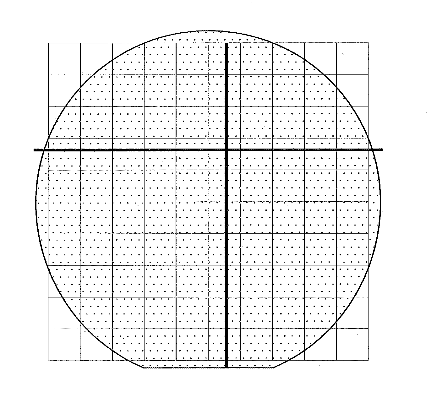
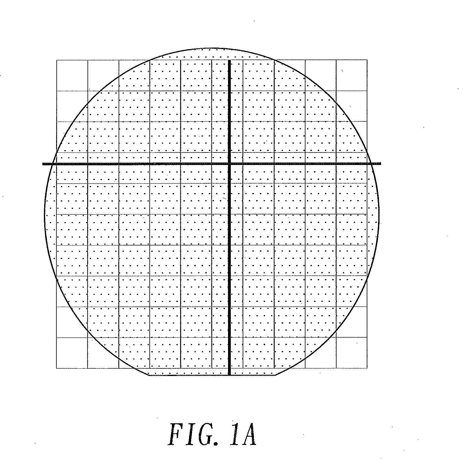
However, the patterns created by the stepper have flaws or tolerances in the patterns serious to a degree that those flaws are visible to the naked eye.
On the other hand, the flawed patterns will inevitably result the defects of the sapphire substrate and scratches and grid lines are most common defects found on the substrate.
If the scratches on the defected substrate are too severe, it will penetrate the epitaxial wafer.
Problems related to grid lines can be mainly categorized to grid dislocation, overlap or separation, and would cause serious epitaxial defects.
If the situation is too serious, then the PSS with the defected grid lines will cause a large defective area across the epitaxial wafer.
Eventually, the failed wafer created by the grid lines will be much more than the failed wafer caused by other defects.

Method used


Image

  • Method for fabricating defect free silicon mold insert
  • Method for fabricating defect free silicon mold insert
  • Method for fabricating defect free silicon mold insert

Examples


Embodiment Construction

[0030]As shown in FIG. 2, a method for fabricating defect-free silicon mold insert (S100) includes the steps of providing a mold insert (step S10); creating a photoresist pattern (step S20); Depositing a metal film (step S30); forming a plurality of metal posts (step S40); conducting heating and annealing process (step S50); conducting dry etching (step S60); and removing the metal balls to create the defect-free silicon mold insert (step S70).

[0031]As shown in FIGS. 2 and 3, the step of providing a mold insert (step S10), and the mold insert 10 is used to serve as a substrate on which a pattern is further formed thereon. The mold insert is a hard substrate which is made from a monocrystalline silicon (s-Si), polycrystalline silicon (c-Si), silicon oxide (SiOx), silicon carbide (SiC), aluminum nitride (AlN), alumina (Al2O3), spinel (MgAl2O4), zinc selenide (ZnSe), zinc oxide (ZnO), gallium nitride (GaN), gallium phosphide (GaP), or a combination of more than two of the above-mention...


PUM

PropertyMeasurementUnit
Diameteraaaaaaaaaa
Defectsaaaaaaaaaa

Abstract

The present invention discloses a method for fabricating a default free silicon mold insert. The method includes providing a silicon mold insert substrate, producing a photoresist pattern, coating a metal film, removing the photoresist pattern, performing heating and annealing, performing dry etching, and removing the metal balls so as to fabricate the default free silicon mold insert. The default free silicon mold insert produced by the method of the present invention can be applied to the nonoimprint process in manufacturing epitaxy wafers to microscopicly provide uniform distances of patterns on the silicon mold insert, and macroscopicly eliminate the grid lines on the epitaxy wafers, and enormously raise the throughput of epitaxy wafer productions. With the ease of application, cheap and fully reproducible nature of the default free silicon mold insert, nanoimprint technology can really replace the stepper machines used nowadays for producing default free nanoimprint mold insert.

Description

BACKGROUND OF THE INVENTION[0001]1. Technical Field[0002]The present invention is related to a method for fabricating defect free silicon mold insert, and more particularly to a method for fabricating defect free silicon mold insert used for the nono imprint process in manufacturing epitaxial wafers.[0003]2. Description of Related Art[0004]Patterned sapphire substrate (Patterned Sapphire Substrate, PSS) is generally having its patterns created by means of yellow light manufacturing process. Among all, stepper is the most popular process. However, the patterns created by the stepper have flaws or tolerances in the patterns serious to a degree that those flaws are visible to the naked eye. These flawed patterns are so called grid lines by the manufacturers of the sapphire substrate. On the other hand, the flawed patterns will inevitably result the defects of the sapphire substrate and scratches and grid lines are most common defects found on the substrate. If the scratches on the defe...

Claims


Application Information

Patent Timeline
IPC IPC(8): H01L21/033
CPCH01L21/033G03F7/0002H01L21/0337
Inventor LEE, CHONG-MINGLEE, CHUNG-HUA
Owner NANOCRYSTAL ASIA
Learn More