Semiconductor integrated circuit device
a technology of integrated circuits and semiconductors, applied in the direction of semiconductor devices, basic electric elements, electrical appliances, etc., can solve the problems of increasing the area of the whole integrated circuit, the number of decoupling capacitance elements to be disposed is extremely small, and the latch-up recently becomes a significant problem, so as to achieve the effect of suppressing latch-up without increasing the area of the entire integrated circui
- Summary
- Abstract
- Description
- Claims
- Application Information
AI Technical Summary
Benefits of technology
Problems solved by technology
Method used
Image
Examples
first exemplary embodiment
[0030]Exemplary embodiments of the present disclosure will be described in detail below with reference to the drawings.
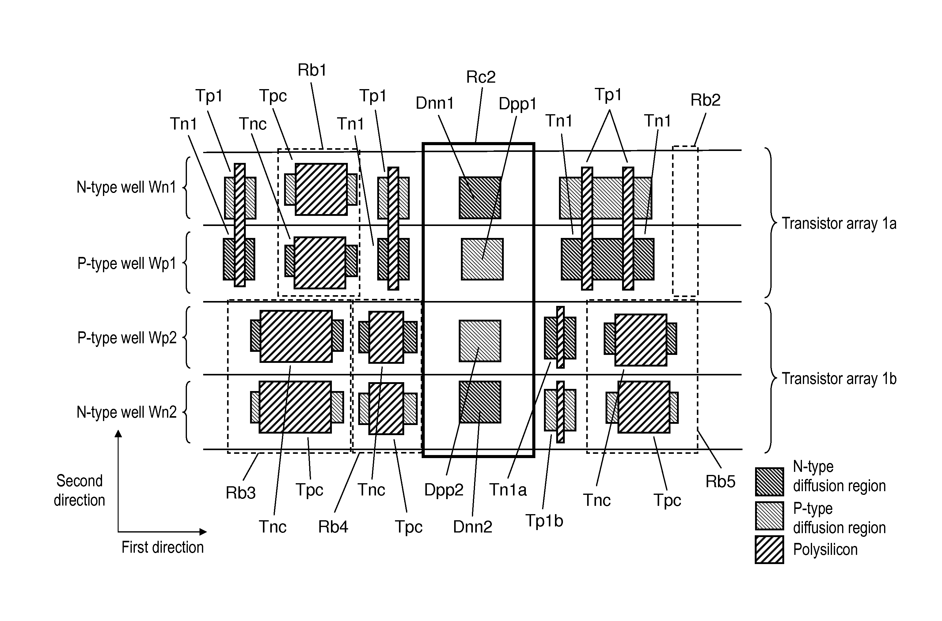
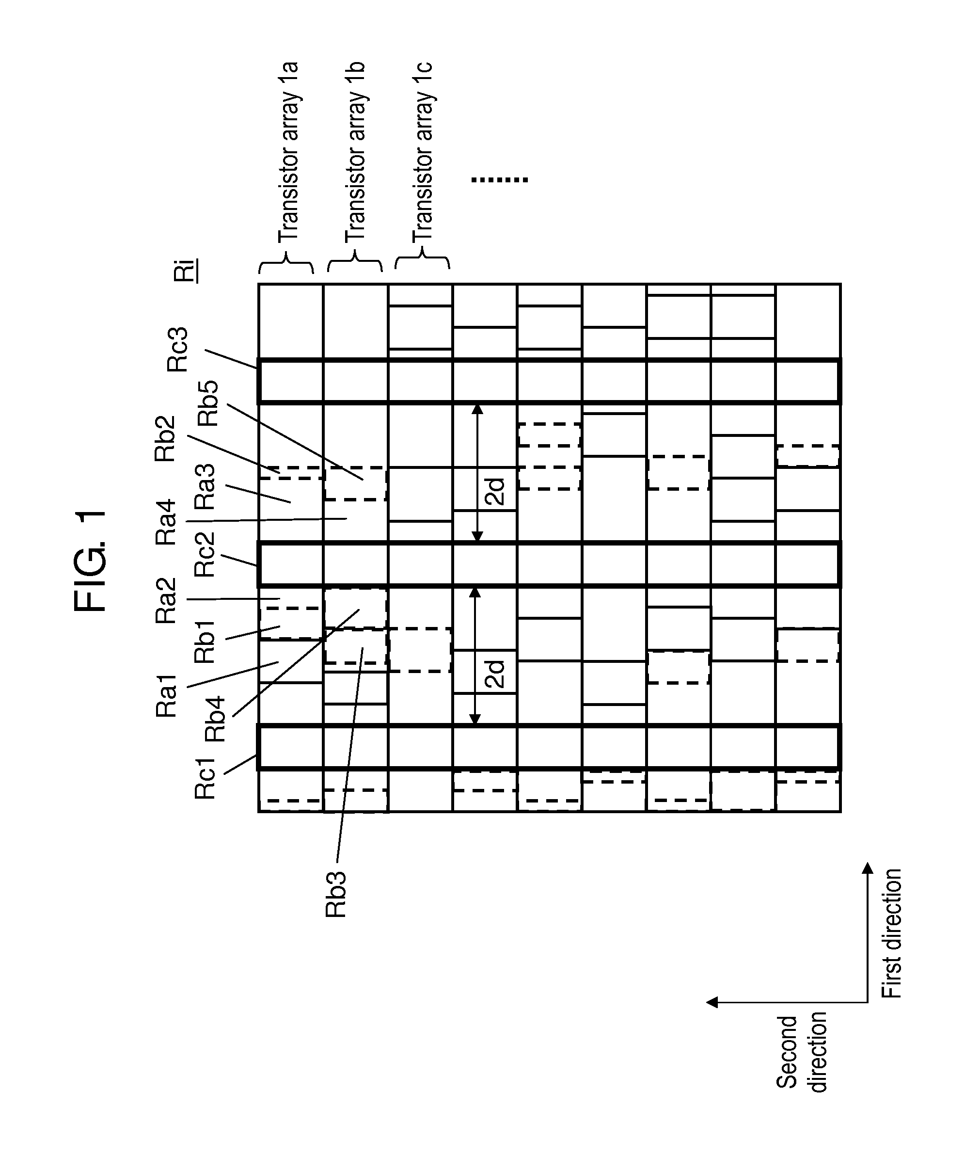
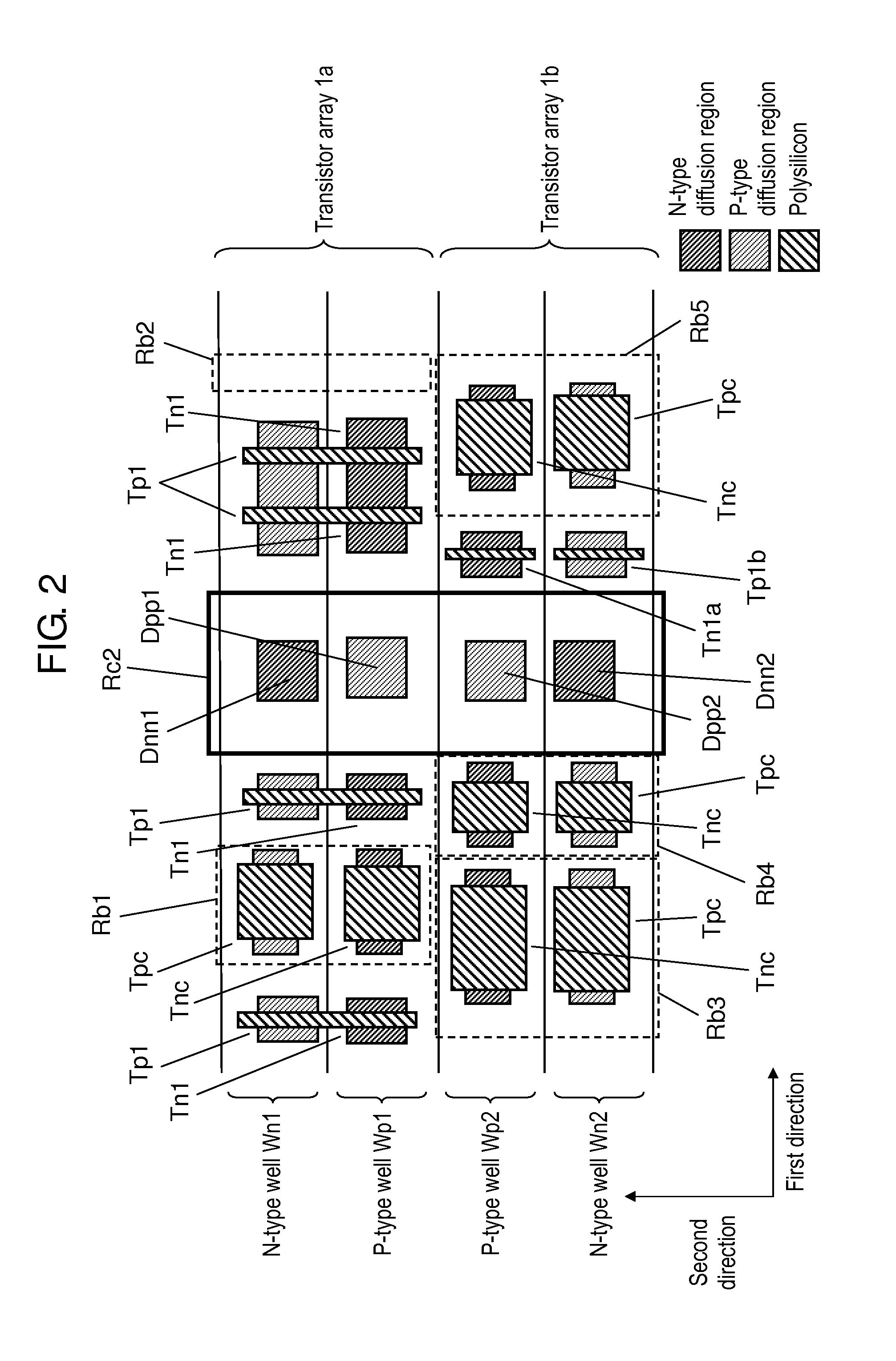
[0031]FIG. 1 is a schematic diagram illustrating a layout pattern of a semiconductor integrated circuit device according to a first exemplary embodiment, and FIG. 2 is a schematic diagram illustrating a layout pattern in which a decoupling capacitance element is disposed in a margin region of the semiconductor integrated circuit device in FIG. 1. FIG. 3 is a schematic diagram illustrating a layout pattern of the semiconductor integrated circuit device according to the first exemplary embodiment.
[0032]As illustrated in FIG. 1, circuit elements are disposed in a first direction, and transistor arrays 1a, 1b, 1c, . . . are formed. Semiconductor integrated circuit Ri is formed by arranging the transistor arrays 1a, 1b, 1c, . . . in the second direction. Substrate contact regions Rc1, Rc2, and Rc3 extend in the second direction in semiconductor integrated circuit Ri, and...
second exemplary embodiment
[0046]A second exemplary embodiment will be described next with reference to FIG. 4. FIG. 4 is a schematic diagram illustrating a layout pattern of a semiconductor integrated circuit device according to the second exemplary embodiment. The different point between the layout pattern illustrated in FIG. 4 and the layout pattern according to the first exemplary embodiment described with reference to FIG. 3 is only margin region Rb3. Therefore, the structure of only margin region Rb3 will be described. The other configurations are identified with the same numerals, and the redundant description will not be made.
[0047]As illustrated in FIG. 4, only transistor Tnc2 serving as the decoupling capacitance is formed on P-type well Wp2 in margin region Rb3, while a pair of transistor Tpc1 serving as the decoupling capacitance and substrate contact Dn1 is disposed on N-type well Wn2 as in FIG. 3. The transistor serving as the decoupling capacitance is composed of a CMOS transistor in the presen...
third exemplary embodiment
[0050]A third exemplary embodiment will next be described with reference to FIG. 5. FIG. 5 is a schematic diagram illustrating a layout pattern of a semiconductor integrated circuit device according to the third exemplary embodiment. The different point between the layout pattern illustrated in FIG. 5 and the layout pattern according to the first exemplary embodiment described with reference to FIG. 3 is only margin region Rb3. Therefore, the structure of only margin region Rb3 will be described. The other configurations are identified with the same numerals, and the redundant description will not be made.
[0051]In the first exemplary embodiment described with reference to FIG. 3, substrate contacts Dp1 and Dn1 are concentrated in margin region Rb3. In the case where the regions of N-type MOS transistor Tnc1 and P-type MOS transistor Tpc1 are large, the distance between substrate contacts Dpp2 and Dnn2 and substrate contacts Dp1 and Dn1 increases, so that the effect of preventing lat...
PUM
 Abstract
Description
Claims
Application Information
 - R&D
- Intellectual Property
- Life Sciences
- Materials
- Tech Scout
- Unparalleled Data Quality
- Higher Quality Content
- 60% Fewer Hallucinations
Browse by: Latest US Patents, China's latest patents, Technical Efficacy Thesaurus, Application Domain, Technology Topic, Popular Technical Reports.
© 2025 PatSnap. All rights reserved.Legal|Privacy policy|Modern Slavery Act Transparency Statement|Sitemap|About US| Contact US: help@patsnap.com


