Lead pin for package substrate
a technology of lead pins and substrates, applied in the direction of application, superimposed coating process, coatings, etc., can solve the problems of lead pin inclination, high cost, and high cost, so as to prevent the pollution of the connection pin, increase bonding efficiency, and increase the contact area
- Summary
- Abstract
- Description
- Claims
- Application Information
AI Technical Summary
Benefits of technology
Problems solved by technology
Method used
Image
Examples
second embodiment
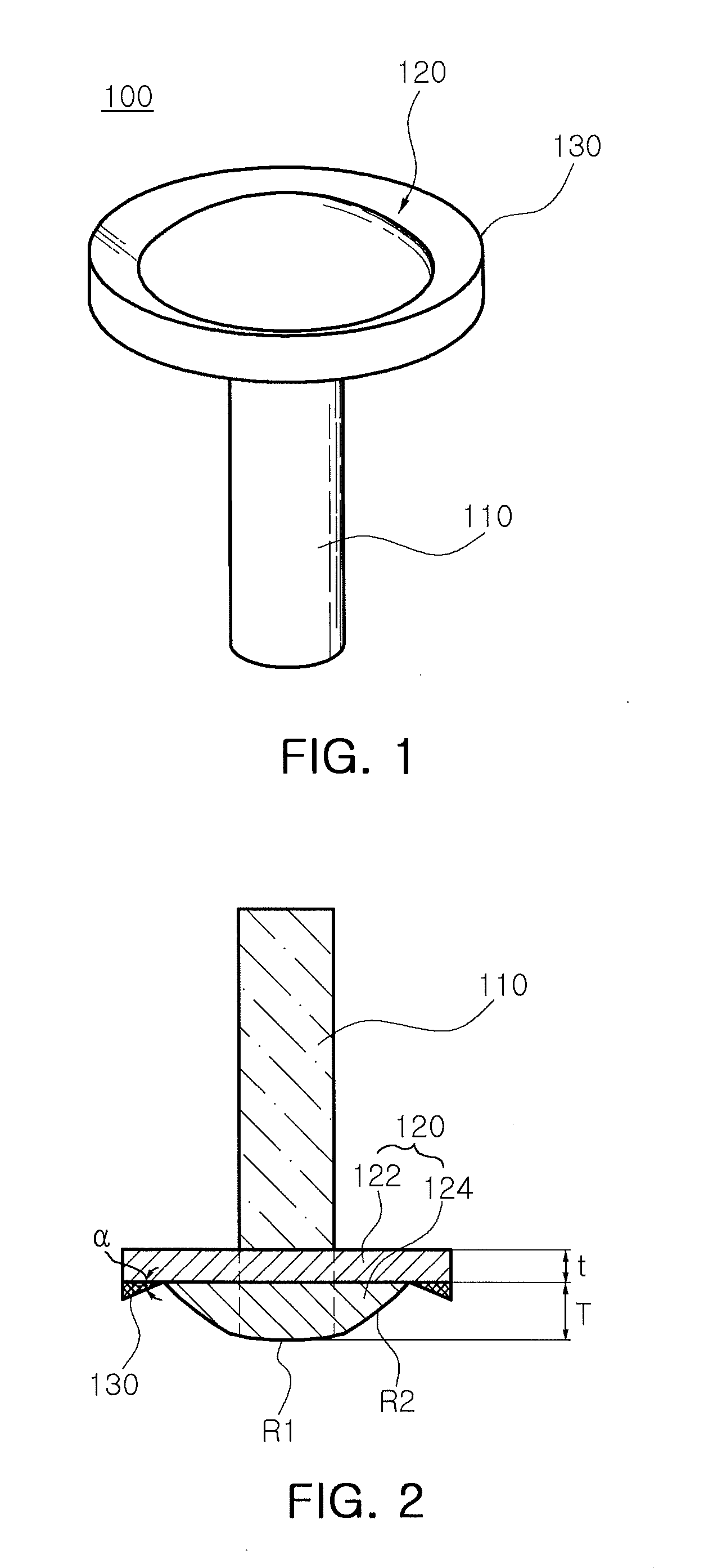
[0079]FIG. 6 is a cross-sectional view explaining a lead pin for a package substrate according to the present invention.
[0080]Referring to FIG. 6, the lead pin for the package substrate may include a connection pin 210, a head part 220, and a barrier part 230.
[0081]At this time, the connection pin 210 and the head part 220 are substantially the same as those shown in the previous embodiment, such that the detailed description thereof may be omitted.
[0082]The barrier part 230 is formed so as to be positioned on a side surface of a flange 222, wherein it may have a shape projected from the side surface.
[0083]Also, the barrier part 230 may be projected, in a tapered shape, to the one edge of the flange part 222. Therefore, the barrier part 230 allows the length of the flange part 222 to be extended in the edge side.
[0084]Therefore, the lead pin for the package substrate according to the present embodiment includes the barrier part 230 that blocks the path of the solder paste so as to p...
third embodiment
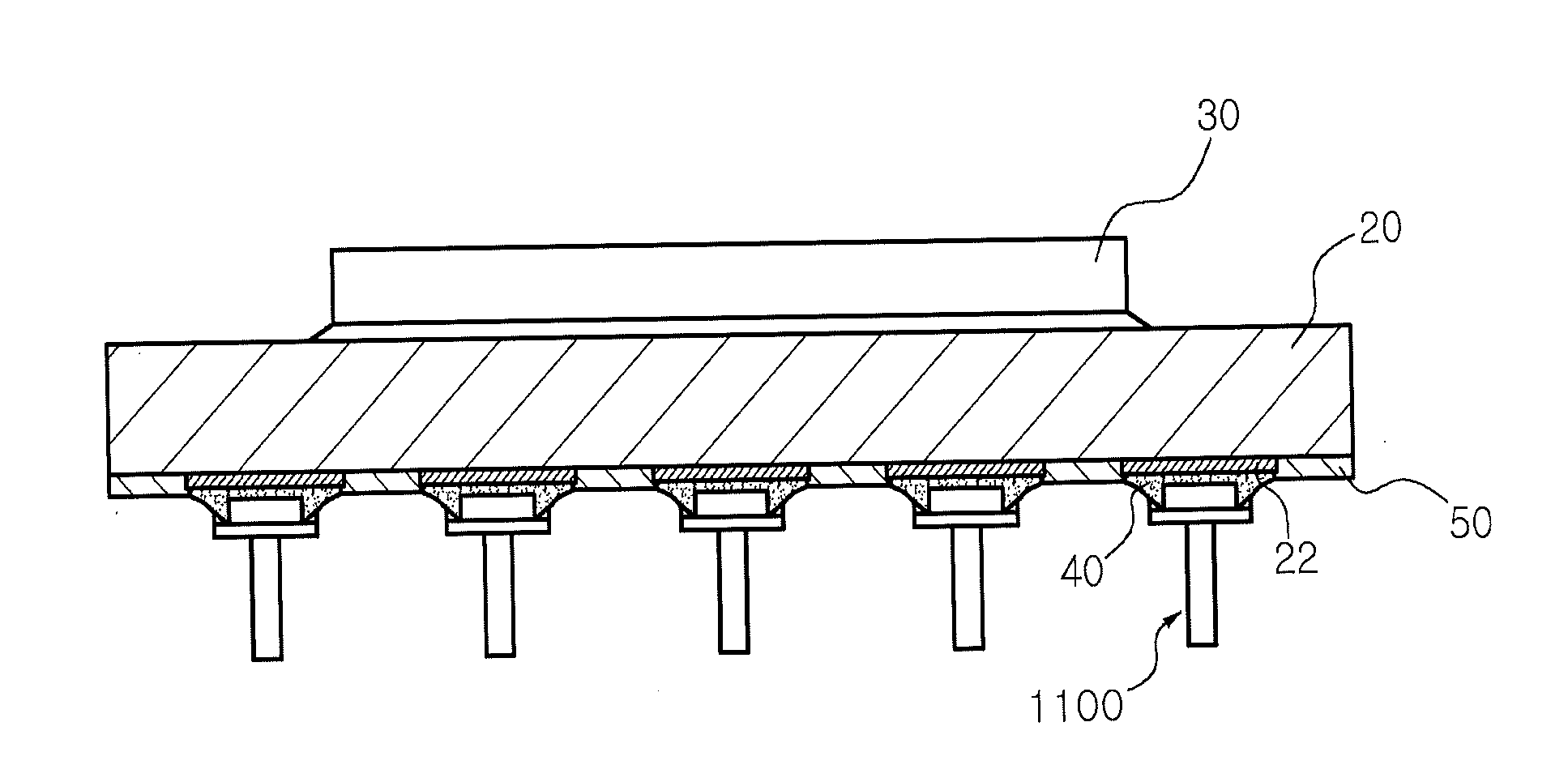
[0085]FIG. 7 is a side cross-sectional view explaining a semiconductor package according to the present invention, and FIG. 8 is a partial cross-sectional view explaining a state in which the lead pin of FIG. 7 is mounted on a substrate.
[0086]Referring to FIGS. 7 and 8, the semiconductor package 10 may include a substrate part 20 and a lead pin 1100.
[0087]A semiconductor chip 30 is electrically connected to the surface of the substrate part 20, wherein the substrate part 20 may use an organic substrate or a ceramic substrate such as a low temperature co-fired ceramic (LTCC).
[0088]In addition, a pad part 22 that is electrically connected to the lead pin 1100 may be formed on the bottom surface of the substrate part 20 and a photoresist layer 50 may be provided around the pad part 22. Also, the substrate part 20 may be manufactured in a plurality of layers, and circuit patterns that electrically connect the plurality of layers may be formed therein.
[0089]Therefore, the semiconductor c...
fourth embodiment
[0109]FIGS. 11 and 12 are cross-sectional views explaining a plane part and a barrier part of a lead pin according to the present invention.
[0110]Referring to FIG. 11, the lead pin may include a connection pin 1210, a head part 1220, and a barrier part 1230.
[0111]Herein, the connection pin 1210 and the barrier part 1230 according to the present embodiment are substantially the same as those shown in the previous embodiment, such that the detailed description thereof may be omitted.
[0112]At this time, the barrier part 1230 and a plane part 1224 may be spaced apart from each other on a flange part 1222. At this time, the barrier part 1230 and the plane part 1224 may be connected to each other and the barrier part 1230 and the plane part 1224 may be spaced apart from each other by processing portions adjacent to the plane part 1224.
[0113]Referring to FIG. 12, it may be appreciated that a portion in which the plane part 1324 and the barrier part 1330 contact each other is formed so as t...
PUM
 Abstract
Description
Claims
Application Information
 - R&D
- Intellectual Property
- Life Sciences
- Materials
- Tech Scout
- Unparalleled Data Quality
- Higher Quality Content
- 60% Fewer Hallucinations
Browse by: Latest US Patents, China's latest patents, Technical Efficacy Thesaurus, Application Domain, Technology Topic, Popular Technical Reports.
© 2025 PatSnap. All rights reserved.Legal|Privacy policy|Modern Slavery Act Transparency Statement|Sitemap|About US| Contact US: help@patsnap.com


