
Organic light emitting element, organic light emitting display device, and method of manufacturing the organic light emitting display device

a technology of organic light emitting elements and display devices, which is applied in the direction of solid-state devices, semiconductor devices, thermoelectric devices, etc., can solve the problems of shortened life of oled elements, undesirable color shifts, and difficulty in adjusting color coordinates, so as to reduce the efficiency of blue light and reduce the efficiency of oled elements

Active Publication Date: 2014-07-03
LG DISPLAY CO LTD
View PDF9 Cites 91 Cited by
  • Summary
  • Abstract
  • Description
  • Claims
  • Application Information

AI Technical Summary

Benefits of technology

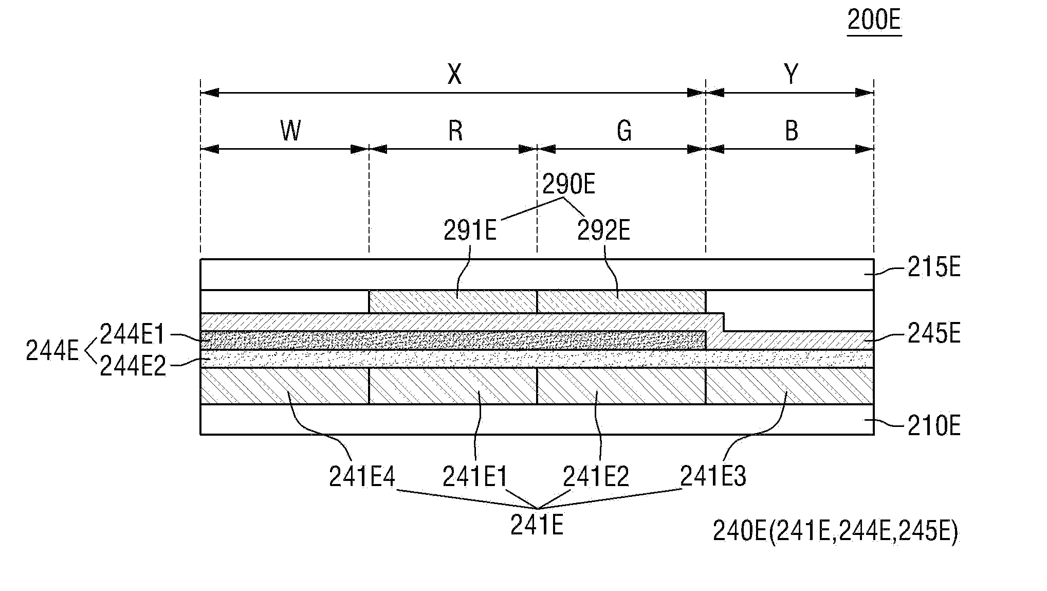
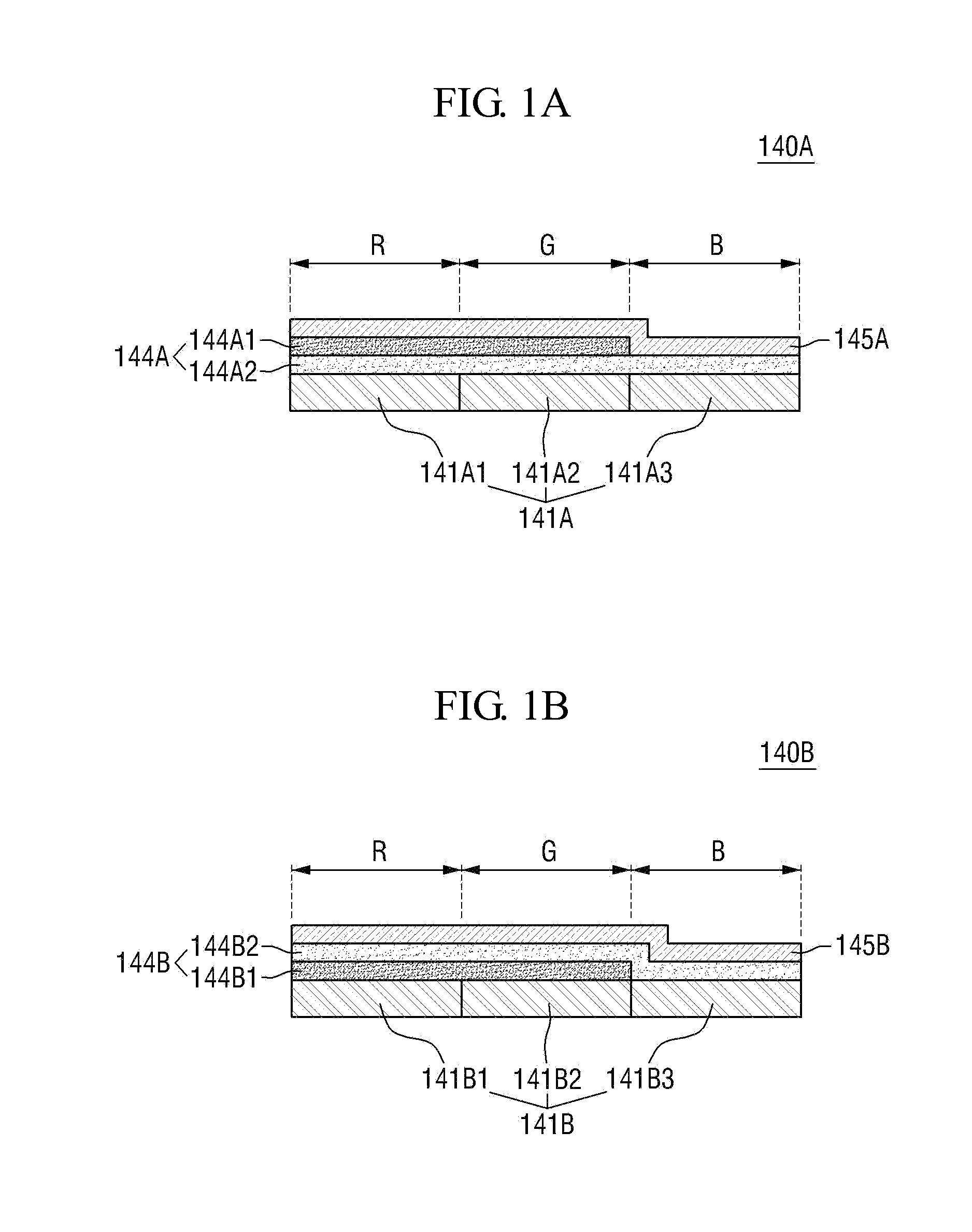
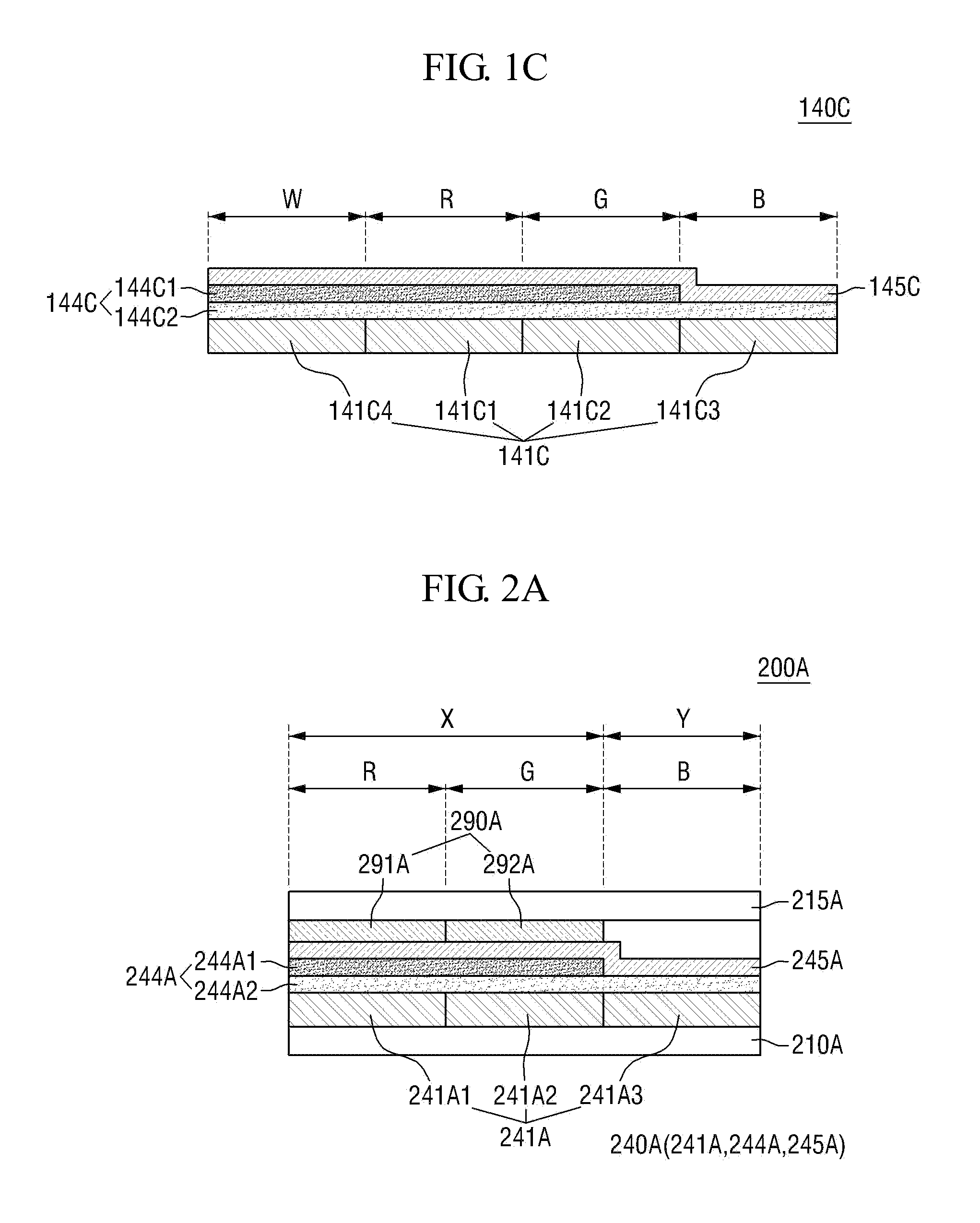
The invention provides a display device with improved efficiency and increased lifespan. It includes a multi-layered emission layer structure with a blue electroluminescent layer and a complementary EL layer. The blue EL layer emits blue light and the complementary EL layer emits light that complements the blue light to form substantially white light. This design ensures that the white light passes through color filters without being absorbed, thereby improving the efficiency of the OLED element. The order in which the blue EL layer and the complementary EL layer are disposed within the multi-layered emission layer structure can vary depending on the emission type of the OLED element employed by the display device.

Problems solved by technology

However, this type of OLED device (referred hereinafter as “RGB type”) requires the OLED elements to be disposed according to the sub pixel design of the display device, thereby severely limiting its application.
Such increase in current density, however, leads to shortened lifetime of OLED element and undesirable color shifts as the display device ages.
However, not only is the algorithm for correcting color coordinates require very complicated arithmetic operations, this method often involves increasing the current level at the white sub pixel region as well as some of the other pixel regions in order to correct the overall color saturation.
This results in increased power consumption of the entire panel and reduced lifespan of the EL layer.
Using a low-power driving algorithm following the aforementioned calibration significantly complicates the overall operation.
Even if such algorithms can be performed, other side effects may occur.

Method used


Image

  • Organic light emitting element, organic light emitting display device, and method of manufacturing the organic light emitting display device
  • Organic light emitting element, organic light emitting display device, and method of manufacturing the organic light emitting display device
  • Organic light emitting element, organic light emitting display device, and method of manufacturing the organic light emitting display device

Examples


Embodiment Construction

[0050]The present invention, which provides an organic light emitting element with improved luminance efficiency and lifetime, and methods of fabricating such an organic light emitting element, will now be described in greater detail by referring to the following discussion and drawings that accompany the present application.

[0051]In the following description, numerous specific details are set forth, such as particular structures, components, materials, dimensions, processing steps and techniques, in order to provide an understanding of the various embodiments of the present disclosure. In other instances, well-known structures or processing steps have not been described in detail in order to avoid obscuring the present disclosure.

[0052]It will be understood that when an element as a layer, region or substrate is referred to as being “on” another element, it can be directly on the other element or intervening elements may also be present. In contrast, when an element is referred to ...


PUM


Abstract

A white organic light emitting element, a white organic light emitting display device, and a method of manufacturing the white organic light emitting element are provided. The organic light emitting element includes a multi-layered emission layer structure. The multi-layered emission layer structure includes a first electroluminescent layer and a second electroluminescent layer that are arranged to overlap at first area of the white organic light emitting element. The lights from the first and second electroluminescent layers collectively form white light. Among the first and second electroluminescent layers, one of the EL layers is extended out to the second area of the white organic light emitting element. A plurality of color filter elements are used to filter the white light to generate colored lights at the corresponding sub pixel regions.

Description

CROSS-REFERENCE TO RELATED APPLICATION[0001]This application claims priority to and the benefit of Korean Patent Application No. 2012-0155868, filed on Dec. 28, 2012, the disclosure of which is incorporated herein by reference in its entirety.BACKGROUND[0002]1. Field of the Invention[0003]The present invention relates to an organic light emitting element (referred hereinafter as “OLED element”) with improved light output rate, power consumption and lifespan and organic light emitting device employing the OLED element, as well as a method of manufacturing such OLED element and device.[0004]2. Discussion of Related Art[0005]An organic light emitting diode device (sometimes referred to as OLED device) is a self-emitting display device. Unlike the liquid crystal display (LCD) display device, it does not require an additional light source, and thus the OLED device can have much thinner and lighter profile than the LCD display device. Not only is the OLED device consumes less power than t...

Claims


Application Information

Patent Timeline
IPC IPC(8): H01L27/32H01L51/56
CPCH01L27/322H01L51/56H01L27/3209H10K59/32H10K59/351H10K59/38H10K50/13H10K50/19G02B5/20
Inventor HEO, JOONYOUNG
Owner LG DISPLAY CO LTD
Learn More