
Calibration schemes for charge-recycling stacked voltage domains

a technology of stacked voltage domain and voltage domain, which is applied in the direction of power consumption reduction, pulse technique, instruments, etc., can solve the problems of power consumption, voltage levels supplied to the circuits are being reduced, and the drivers of the first voltage domain are strong, so as to reduce the effect of reducing the strength of the drivers of the first voltage domain

Active Publication Date: 2014-06-26
GLOBALFOUNDRIES US INC
View PDF0 Cites 16 Cited by
  • Summary
  • Abstract
  • Description
  • Claims
  • Application Information

AI Technical Summary

Benefits of technology

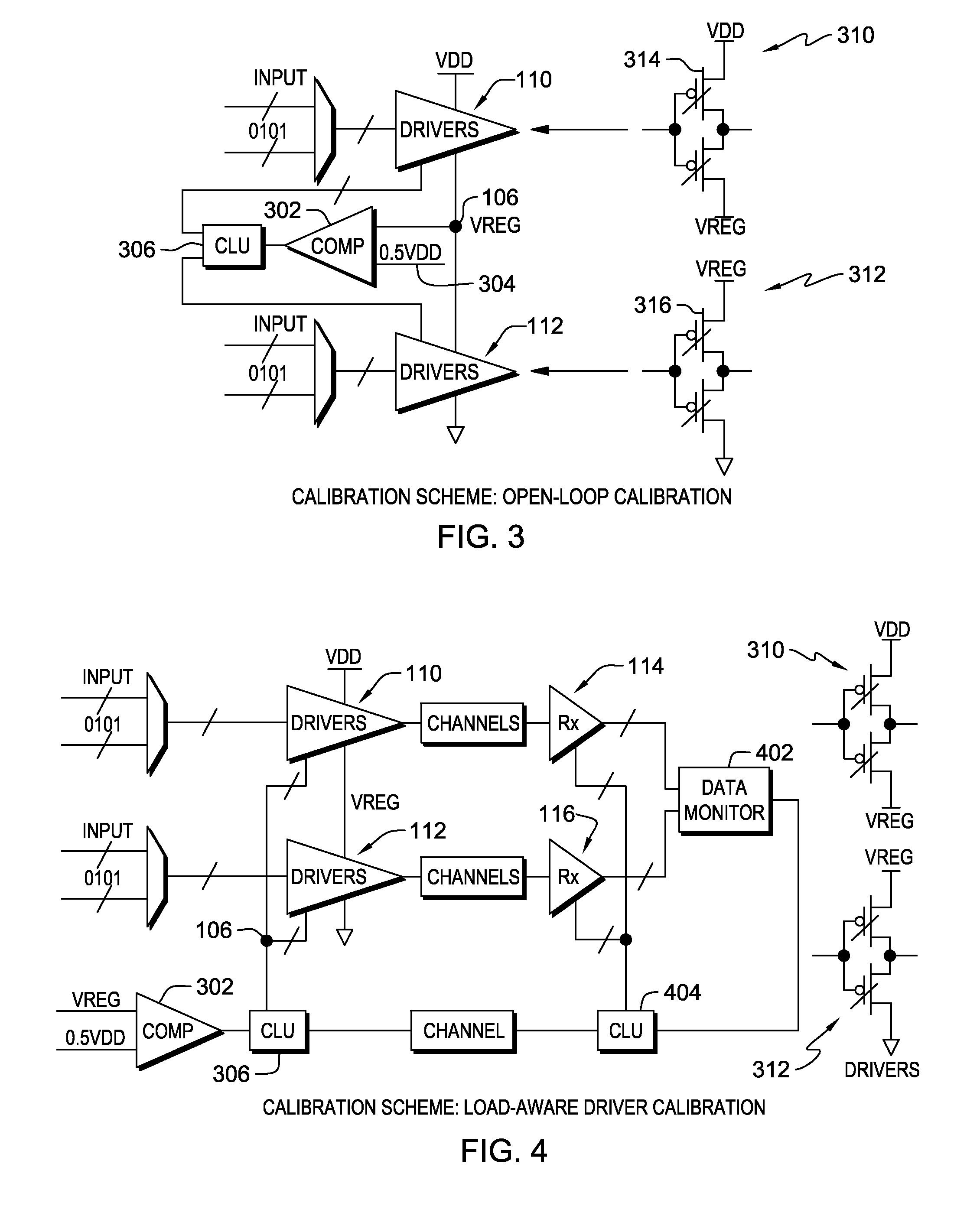
The patent describes a technique to adjust the strengths of drivers in a circuit. This is done by detecting the size of a specified data eye for a group of receivers and comparing it to a predetermined value. By reducing or increasing the strengths of the drivers, the circuit can better control the data transfer.

Problems solved by technology

In the design and operation of integrated circuits, power consumption is a major concern.
As a result of the devices on the circuits becoming smaller and of the higher performance requirements for the circuits, the circuits, or chips, are consuming more power, and the voltage levels supplied to the circuits are being reduced.
This leads to a significant growth in the currents needed to operate the devices on the circuits.
Among various circuit blocks in an I / O system, the signaling power dissipated on the channel consumes a big part of the overall I / O power.
However, the I / O performance can be adversely affected due to chip process variations, supply voltage fluctuations and temperature deviations along the I / O bus.

Method used


Image

  • Calibration schemes for charge-recycling stacked voltage domains
  • Calibration schemes for charge-recycling stacked voltage domains
  • Calibration schemes for charge-recycling stacked voltage domains

Examples


Embodiment Construction

[0026]Disclosed herein is a low voltage signaling technique for integrated circuit systems that substantially reduces I / O power through the use of charge recycling stacked voltage domains.

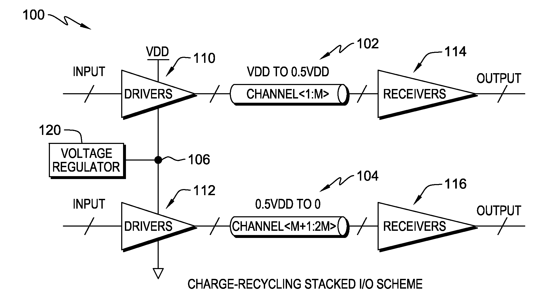
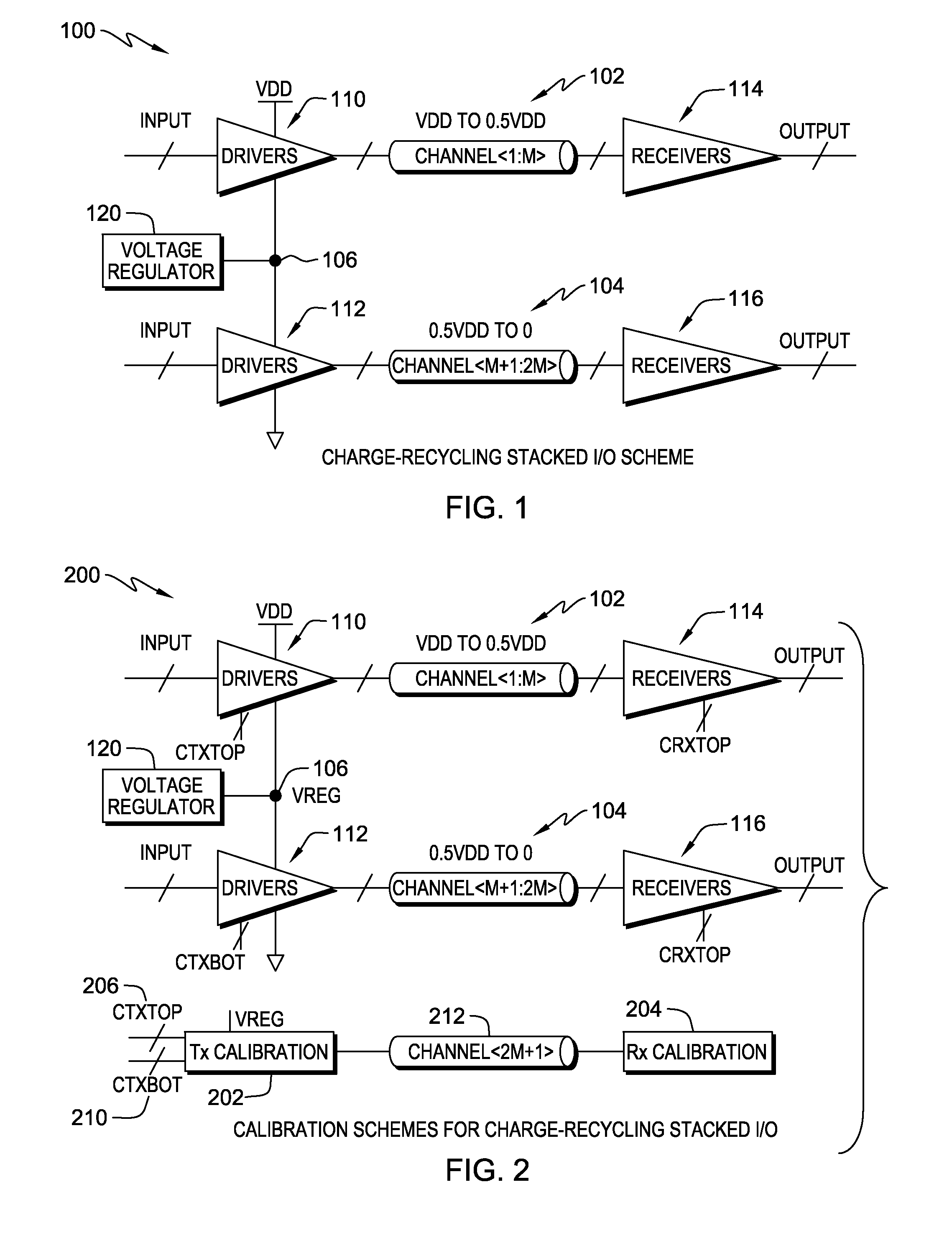
[0027]FIG. 1 shows an input-output circuit having a charge-recycling stacked I / O scheme. FIG. 1 shows, more particularly, a two stack circuit 100 comprising domains 102 and 104, with a mid supply node 106 between the two domains. Two groups of drivers are stacked between the supply voltage VDD and ground: M drivers 110 on the top domain 102 and M drivers 112 on the bottom domain 104 for a 2M-bit data bus. When the average current from the top drivers is equal to the average current from the bottom drivers, the mid-supply node VREG 106 is equal to 0.5 VDD, leading to a 0.5 VDD signal swing for both the top and bottom I / O domains 102 and 104.

[0028]In the operation of circuit 100, as the potential of the electrons decrease from VDD to VREG, that energy is used to perform logic in domain 102. The elect...


PUM


Abstract

A method and system are disclosed for calibrating a mid-voltage node in an integrated circuit including an input-output circuit having charge-recycling stacked voltage domains including at least first and second voltage domains. In one embodiment, the method comprises transmitting data through the input-output circuit, including transmitting a first portion of the data across the first voltage domain, and transmitting a second portion of the data across the second voltage domain. The method further comprises measuring a specified characteristic of the data transmitted through the input-output circuit; and based on the measured specified characteristic, adjusting a voltage of said mid-voltage node to a defined value. The voltage of the mid-voltage node may be adjusted to accomplish a number of objectives, for example, to achieve a desired trade-off between power and performance, or so that the two voltage domains have the same performance.

Description

STATEMENT OF GOVERNMENT INTEREST[0001]This invention was made with Government support under Contract No.: HR0011-09-C-0002 (Defense Advanced Research Projects Agency (DARPA)). The Government has certain rights in this invention.BACKGROUND OF THE INVENTION[0002]This invention generally relates to integrated circuits having charge-recycling stacked voltage domains. More specifically, the invention relates to calibration schemes for such stacked voltage domains.[0003]In the design and operation of integrated circuits, power consumption is a major concern. As a result of the devices on the circuits becoming smaller and of the higher performance requirements for the circuits, the circuits, or chips, are consuming more power, and the voltage levels supplied to the circuits are being reduced. This leads to a significant growth in the currents needed to operate the devices on the circuits.[0004]In on-chip and inter-chip data communication systems where high data bandwidth is required, power...

Claims


Application Information

Patent Timeline
Patent Type & Authority Applications(United States)
IPC IPC(8): G05F1/46
CPCG05F1/462G05F1/56H03K5/08H03K19/0019H03K19/017509
Inventor FRIEDMAN, DANIELLIU, YONGTIERNO, JOSE A.
Owner GLOBALFOUNDRIES US INC
Learn More