


Quick Research
Generate reliable direction feasibility study reports for your R&D in just a few steps.

Technical Q&A
Discover and master advanced knowledge NOW. Basics, ideas, possibilities, all at once.

Find Solutions
As an expert in R&D theories, this can generate solutions to your technical problems instantly.

Evaluate Feasibility
Analyze your overall solution with one click, know your potential R&D risks in advance.

Monitor Landscape
Get weekly tech updates, stay abreast of the latest tech innovations and key insights.
Integrated circuits and methods for fabricating integrated circuits with silicide contacts on non-planar structures
- Summary
- Abstract
- Description
- Claims
- Application Information
AI Technical Summary
Benefits of technology
Problems solved by technology
Method used
Image

Examples
Embodiment Construction
[0012]The following detailed description is merely exemplary in nature and is not intended to limit integrated circuits or the methods for fabricating integrated circuits as claimed herein. Furthermore, there is no intention to be bound by any expressed or implied theory presented in the preceding technical field, background or brief summary, or in the following detailed description.
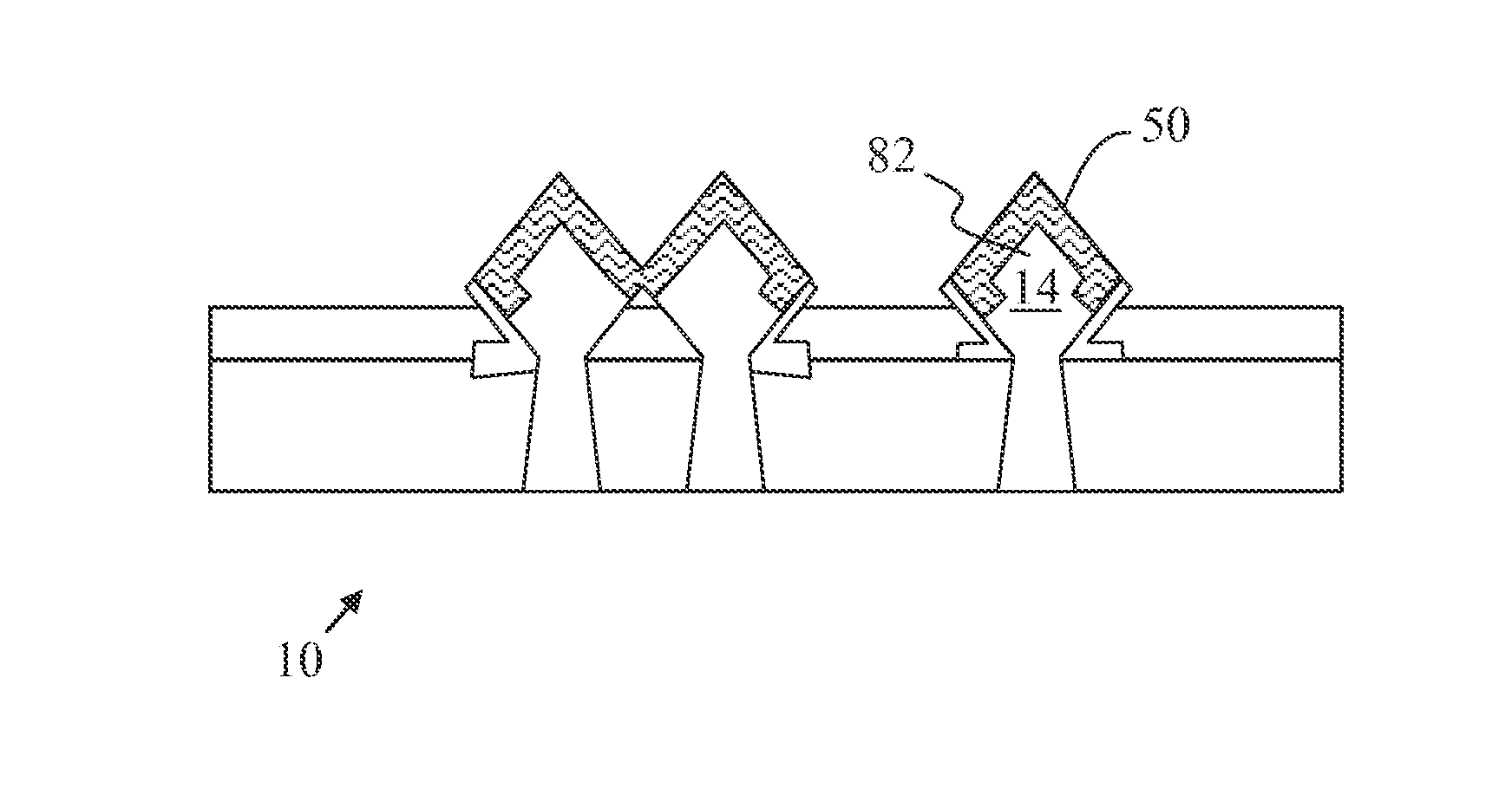
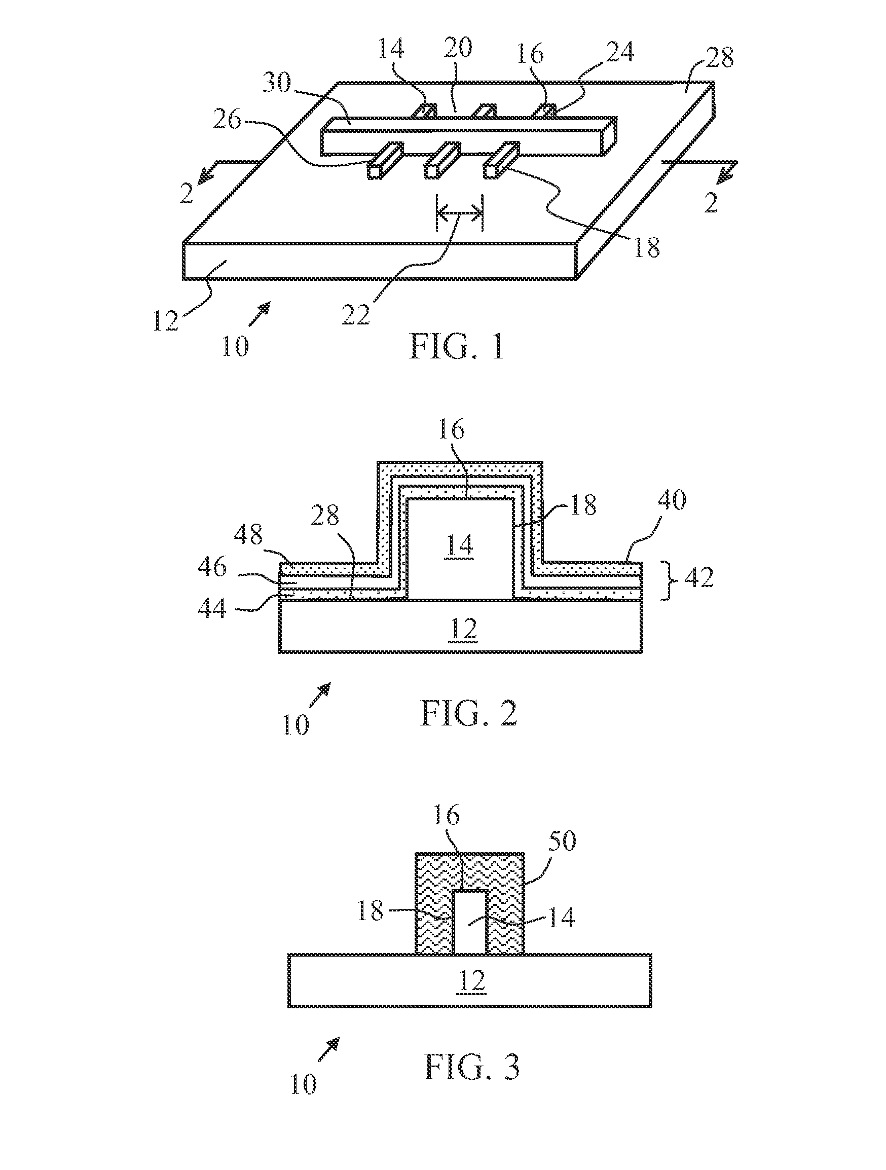
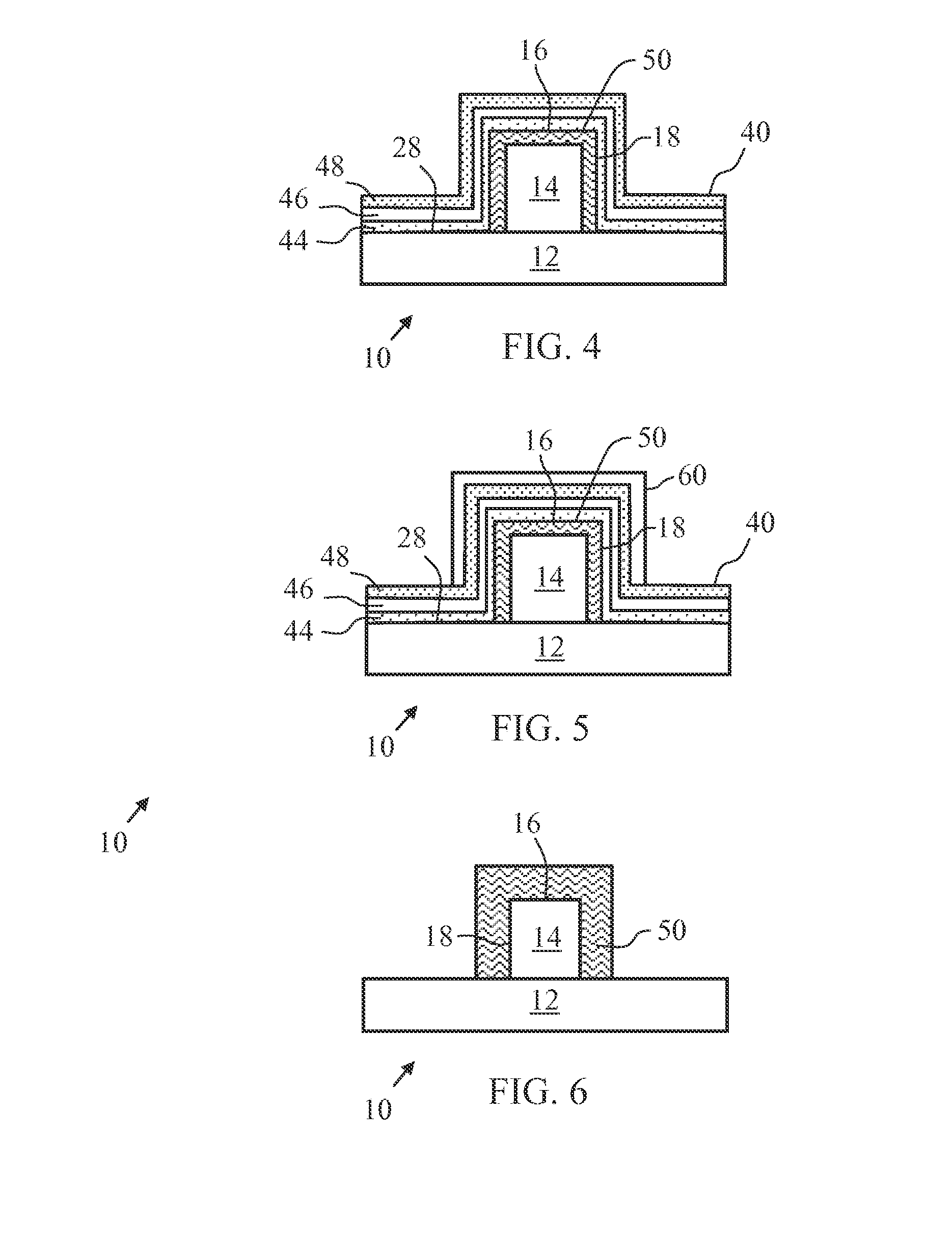
[0013]In accordance with the various embodiments herein, integrated circuits and methods for fabricating integrated circuits with silicide contacts on non-planar structures are provided. Problems faced by conventional processes when forming contacts on non-planar structures may be avoided. In order to avoid consuming the fin, the silicide must be extremely thin. Further, in order to provide sufficient contact area, the silicide must form along the sidewalls of the non-planar fins. It is contemplated herein that metal silicide material be conformally deposited on the sidewalls of non-planar structures in ...
PUM
 Abstract
Description
Claims
Application Information
 - R&D Engineer
- R&D Manager
- IP Professional
- Industry Leading Data Capabilities
- Powerful AI technology
- Patent DNA Extraction
Browse by: Latest US Patents, China's latest patents, Technical Efficacy Thesaurus, Application Domain, Technology Topic, Popular Technical Reports.
© 2024 PatSnap. All rights reserved.Legal|Privacy policy|Modern Slavery Act Transparency Statement|Sitemap|About US| Contact US: help@patsnap.com