
Display device and driving method of the same

a technology of a display device and a driving method, which is applied in the direction of instruments, computing, electric digital data processing, etc., can solve the problems of non-uniformity of luminance, production cost increase, and difficulty in implementing images with accurate luminance, so as to improve the response waveform, improve the uniformity of images, and improve the effect of luminan

Active Publication Date: 2014-05-22
SAMSUNG DISPLAY CO LTD
View PDF23 Cites 33 Cited by
  • Summary
  • Abstract
  • Description
  • Claims
  • Application Information

AI Technical Summary

Benefits of technology

The present invention relates to a display panel and display device that can improve display quality and response waveform. The invention includes a pixel circuit that applies an on-bias voltage to a driving transistor, which is not possible in conventional display devices. This improves the driving process and prepares the circuit for high-resolution and high-speed driving. The invention also provides a simplified layout design without adding a separate voltage wire circuit, ensuring an aperture ratio and manufacturing yield. Overall, the invention provides a display panel and display device with improved image quality and response speed.

Problems solved by technology

Particularly, a display device including a large-sized display panel or a high-speed frame driving for driving of the 3D stereoscopic image is required, but since respective periods for initialization of data voltage, compensation of threshold voltage of a driving transistor, writing of data, and light emission are not sufficiently ensured by the high-speed driving mode, it is difficult to implement images having accurate luminance.
Further, in order to solve the problem, various researches and development for a pixel circuit structure, a driving mode, and luminance compensation have been conducted, but since the pixel circuit structure is complicated and power consumption may be increased according to the luminance compensation or the driving mode, adverse effects that production costs increase and non-uniformity of luminance is not improved may occur.

Method used


Image

  • Display device and driving method of the same
  • Display device and driving method of the same
  • Display device and driving method of the same

Examples


Embodiment Construction

[0060]The present invention will be described more fully hereinafter with reference to the accompanying drawings, in which exemplary embodiments of the invention are shown. As those skilled in the art would realize, the described embodiments may be modified in various different ways, all without departing from the spirit or scope of the present invention.

[0061]The drawings and description are to be regarded as illustrative in nature and not restrictive. Like reference numerals designate like elements throughout the specification.

[0062]Throughout this specification and the claims that follow, when it is described that an element is “coupled” to another element, the element may be “directly coupled” to the other element or “electrically coupled” to the other element through a third element. In addition, unless explicitly described to the contrary, the word “comprise” and variations such as “comprises” or “comprising”, will be understood to imply the inclusion of stated elements but no...


PUM


Abstract

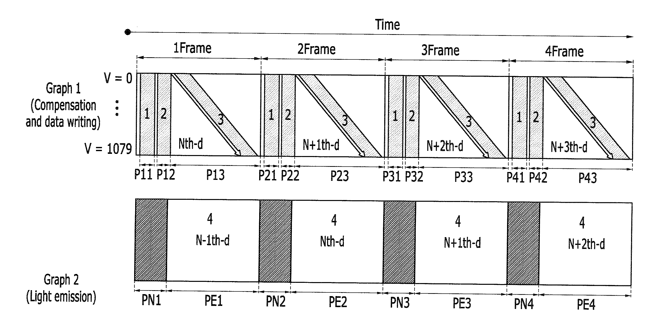
A display device and a driving method thereof. The display device includes a plurality of pixels, each receiving a predetermined on-bias voltage transferred through a data line during one frame, receiving a first image data signal corresponding to the corresponding frame through the data line and storing the same, and emitting light according to a driving current that corresponds to a second image data signal that corresponds to the previous frame of the corresponding frame, and a first period for storing the first image data signal and a second period for light emission according to a driving current corresponding to the second image data signal overlap each other in one frame.

Description

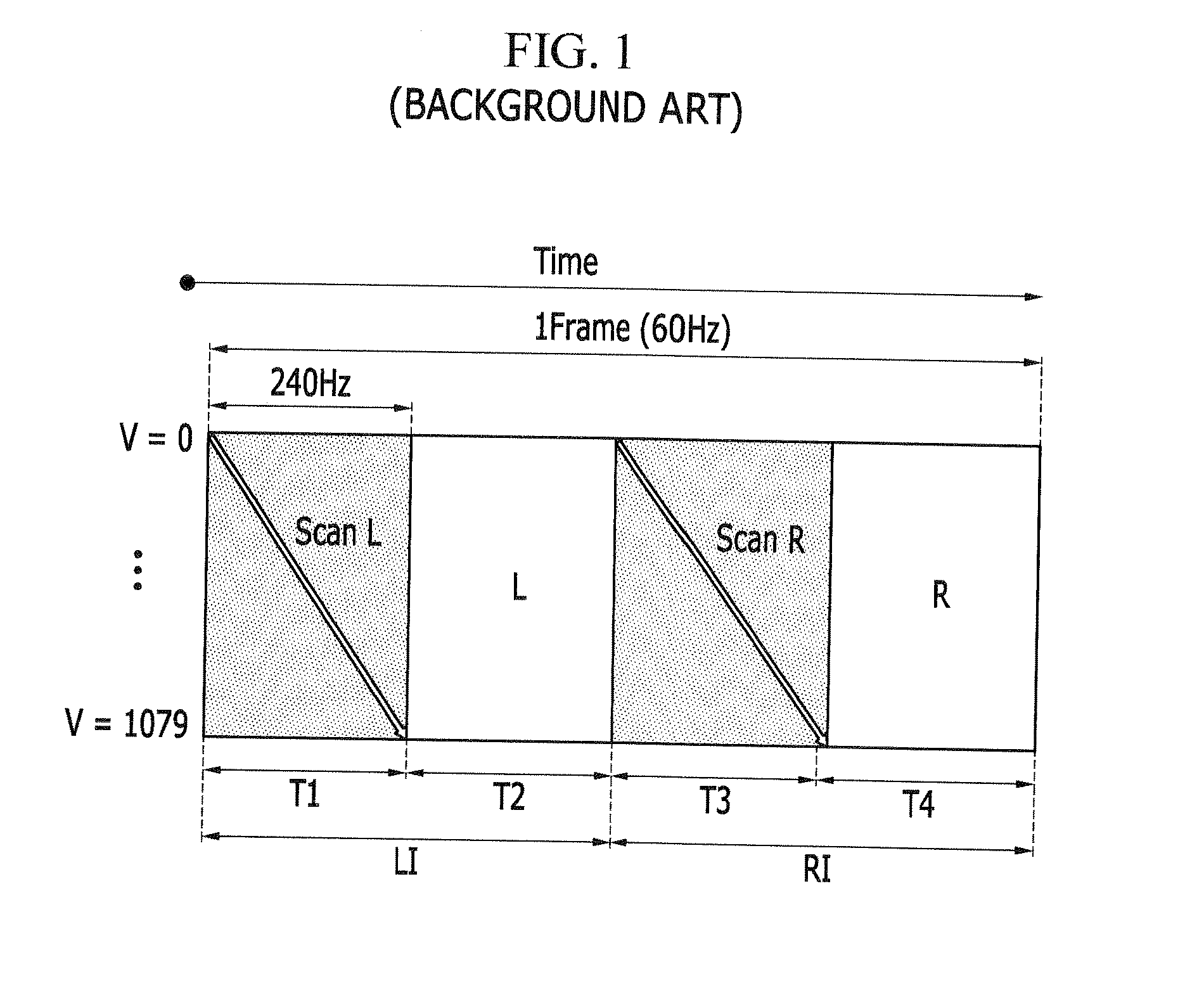
CLAIM OF PRIORITY[0001]This application makes reference to, incorporates the same herein, and claims all benefits accruing under 35 U.S.C. §119 from an application earlier filed in the Korean Intellectual Property Office on the 20 Nov. 2012 and there duly assigned Serial No. 10-2012-0131913.BACKGROUND OF THE INVENTION[0002]1. Field of the Invention[0003]The present invention relates to a display device and a driving method thereof.[0004]2. Description of the Related Art[0005]Recently, a display panel has increased in size and reduced in weight, and a stable driving method of a frame has been developed in order to display an accurate and clear image with high-integration and high-precision of a display device which is required to implement a 3D stereoscopic image.[0006]Particularly, a display device including a large-sized display panel or a high-speed frame driving for driving of the 3D stereoscopic image is required, but since respective periods for initialization of data voltage, ...

Claims


Application Information

Patent Timeline
IPC IPC(8): G09G5/00
CPCG09G3/3233G09G2300/0852G09G2300/0861G09G2310/0216G09G2300/0819H04N13/341H04N13/398G09G3/003G09G3/20
Inventor HAN, SANG-MYEON
Owner SAMSUNG DISPLAY CO LTD
Learn More