Liquid crystal display device and method of manufacturing the same

a technology of liquid crystal display and liquid crystal, which is applied in the direction of semiconductor devices, instruments, optics, etc., can solve the problems that the elements (for example, thin film transistors) included in the lcd device may be seriously damaged, and achieve the effect of reducing the area of the pad portion and being thinner and lighter

Active Publication Date: 2014-03-06
LG DISPLAY CO LTD
View PDF5 Cites 8 Cited by
  • Summary
  • Abstract
  • Description
  • Claims
  • Application Information

AI Technical Summary

Benefits of technology

The invention aims to make LCD devices thinner and lighter by reducing the area of a pad portion.

Problems solved by technology

Due to this, elements (for example, thin film transistors) included in the LCD device may be seriously damaged.

Method used


Image

  • Liquid crystal display device and method of manufacturing the same
  • Liquid crystal display device and method of manufacturing the same
  • Liquid crystal display device and method of manufacturing the same

Examples


Embodiment Construction

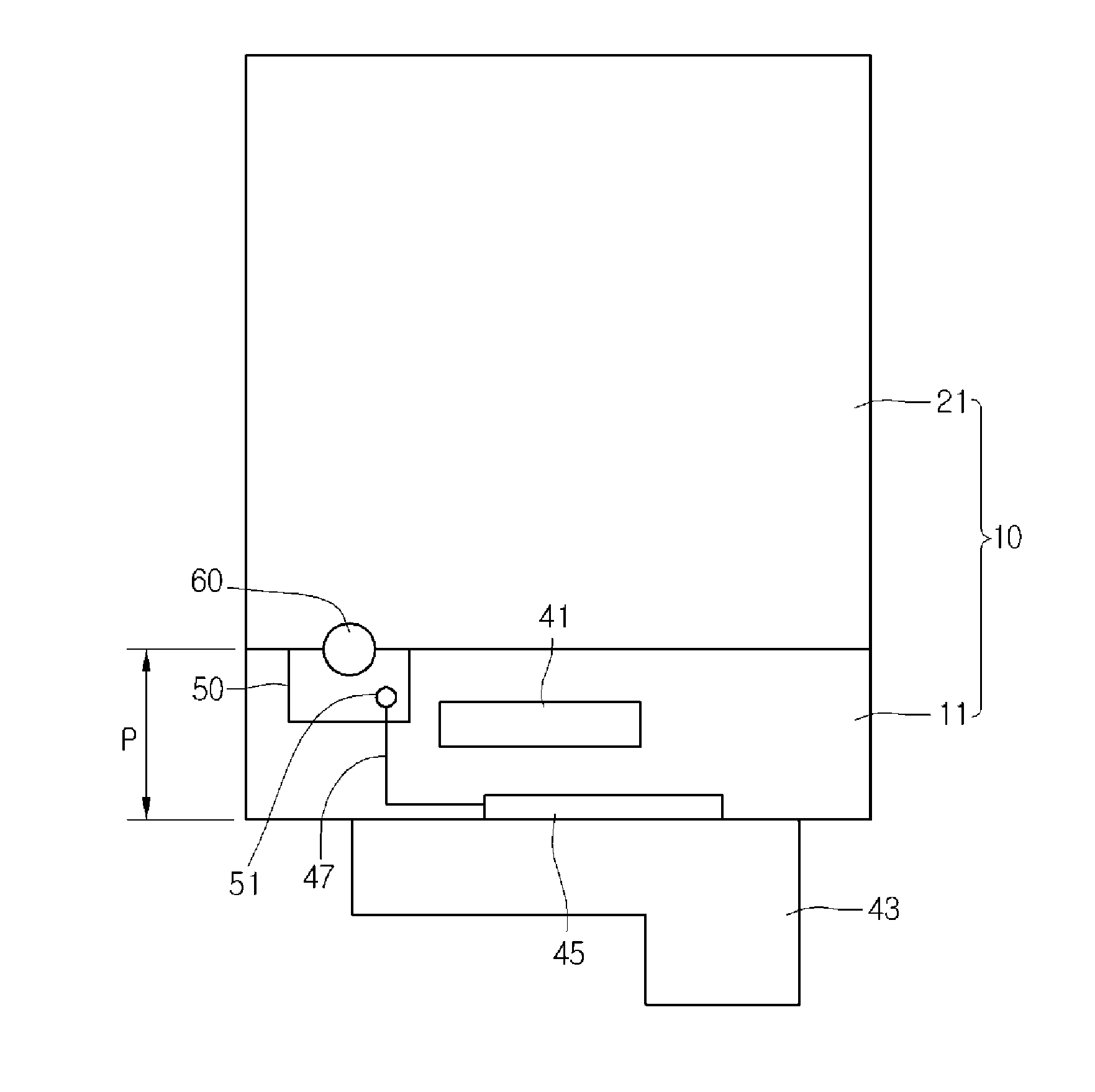
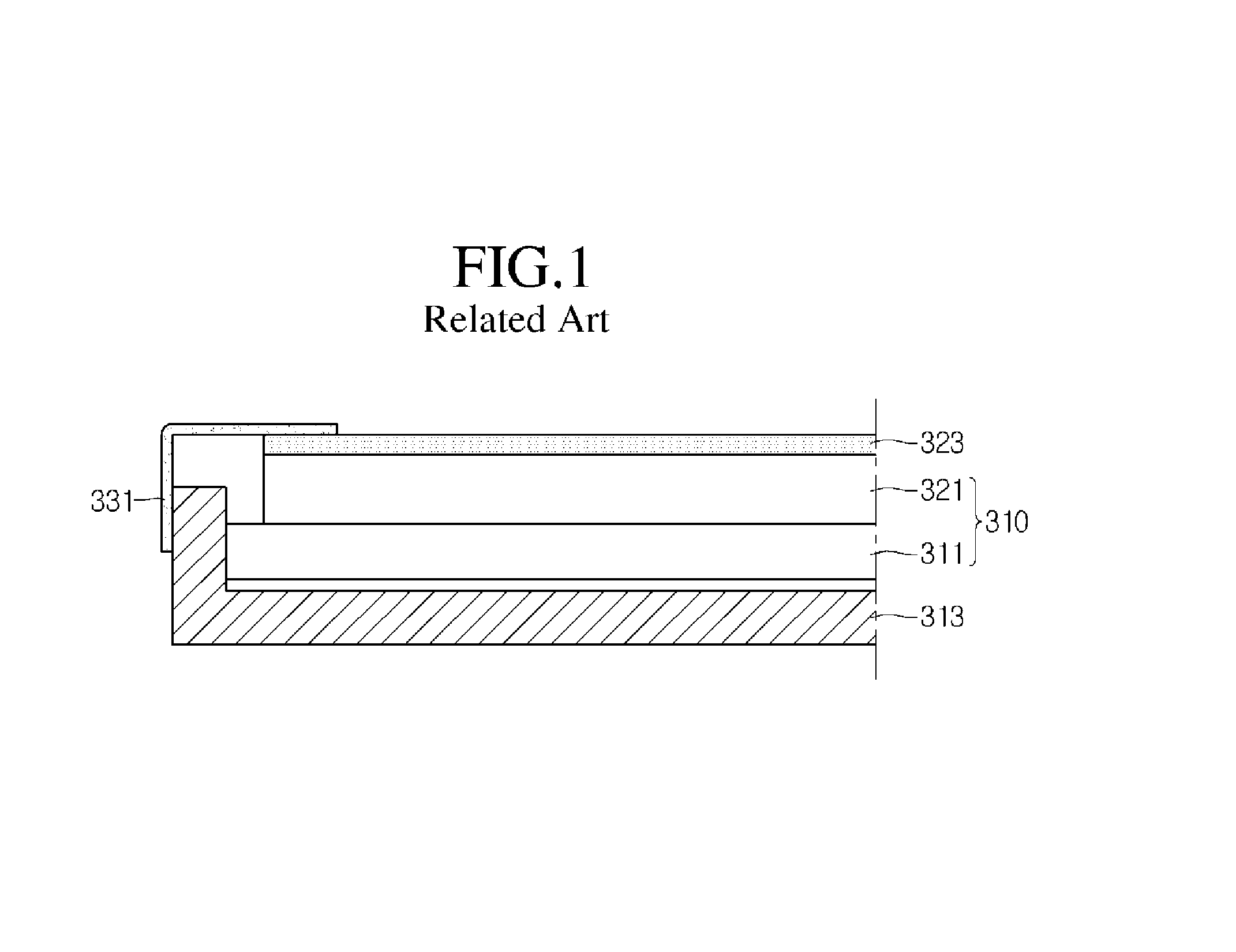
[0028]Reference will now be made in detail to embodiments of the present invention, examples of which are illustrated in the accompanying drawings. In the following description, when a detailed description of well-known functions or configurations related to this document is determined to unnecessarily cloud a gist of the invention, the detailed description thereof will be omitted. The progression of processing steps and / or operations described is an example; however, the sequence of steps and / or operations is not limited to that set forth herein and may be changed as is known in the art, with the exception of steps and / or operations necessarily occurring in a certain order. Like reference numerals designate like elements throughout. Names of the respective elements used in the following explanations are selected only for convenience of writing the specification and may be thus different from those used in actual products.

[0029]In description of embodiments of the present invention,...


PUM

PropertyMeasurementUnit
transparent conductiveaaaaaaaaaa
transparentaaaaaaaaaa
flexibleaaaaaaaaaa

Abstract

A liquid crystal display device and method of manufacturing a liquid crystal display device are provided. The liquid crystal display device includes: a thin film transistor substrate, a color filter substrate on the thin film transistor substrate, a transparent conductive plate on the color filter substrate, a pad portion on the thin film transistor substrate, a static-electricity transmission electrode on a region of the pad portion adjacent to the color filter substrate, a conductive member configured to electrically connect the transparent conductive plate and the static-electricity transmission electrode to each other, and a plurality of lattice patterns on the static-electricity transmission electrode.

Description

CROSS REFERENCE TO RELATED APPLICATION(S)[0001]This application claims the benefit under 35 U.S.C. §119(a) of Korean Patent Application No. 10-2012-0095798, filed on Aug. 30, 2012, the entire disclosure of which is incorporated by reference herein for all purposes.BACKGROUND[0002]1. Technical Field[0003]The present application relates to a liquid crystal display device and method of manufacturing the same.[0004]2. Discussion of the Related Art[0005]As the information society spreads, the requirements for display devices are varied and gradually increasing. In accordance therewith, a variety of display devices such as liquid crystal display (LCD) devices, plasma display panels (PDP), electro-luminescent display (ELD) devices, vacuum fluorescent display (VFD) devices, and so on, have been researched. Furthermore, some display devices already have been applied to many appliances and devices.[0006]More specifically, the LCD devices are rapidly replacing cathode ray tubes (CRTs) and are ...

Claims


Application Information

Patent Timeline
Patent Type & Authority Applications(United States)
IPC IPC(8): G02F1/1343
CPCG02F1/134309G02F1/136204G02F2201/122H01L27/0296H01L2924/0002H01L2924/00G02F1/1345
Inventor JUNG, SUNG HUN
Owner LG DISPLAY CO LTD
Why Eureka
Try Eureka