Method for fabricating patterned silicon nanowire array and silicon microstructure

a silicon nanowire array and microstructure technology, applied in the field of silicon nanowire array and silicon microstructure, can solve the problems of high manufacturing cost, difficult to fabricate difficult to manufacture silicon nanowire array uniformly over a large area for solar panel applications, etc., to achieve easy and low-cost manufacturing

Inactive Publication Date: 2014-01-30
NAT TAIWAN UNIV OF SCI & TECH
View PDF8 Cites 8 Cited by
  • Summary
  • Abstract
  • Description
  • Claims
  • Application Information

AI Technical Summary

Benefits of technology

[0020]In accordance with the fabrication method of the patterned silicon nanowire arrays of the present invention, the oxide layer or the patterned protective layer implemented by the photoresist layer is directly formed between the array of silicon nanowire structures, and then the silicon nanowires which are not protected are etched by the wet etching, thereby easily and low-costly manufacturing the patterned silicon nanowire array. In addition, the present invention is further capable of forming the heterostructures, e.g. growing the carbon nanotubes, on said patterned silicon nanowire array for applying to electrical field emission applications. Finally, the present invention is capable of forming the partial silicon nanowire array on the silicon substrate and then etching the silicon nanowires for achieving the objective that the silicon microstructures with vertical sidewalls can be made by wet etching for any silicon substrate, especially for the (100) monocrystalline silicon.

Problems solved by technology

However, the manufacturing cost thereof is higher, and it is difficult to fabricate the silicon nanowire array uniformly over a large area for solar panel applications.
However, the manner of the single-crystalline growth requires a high-temperature ambient condition above 1000° C. for the growth, so the cost of the fabrication is extremely high.
However, the processes of this fabrication manner are complex, and quality of the patterned silicon nanowire array made thereby is poor.

Method used


Image

  • Method for fabricating patterned silicon nanowire array and silicon microstructure
  • Method for fabricating patterned silicon nanowire array and silicon microstructure
  • Method for fabricating patterned silicon nanowire array and silicon microstructure

Examples


Embodiment Construction

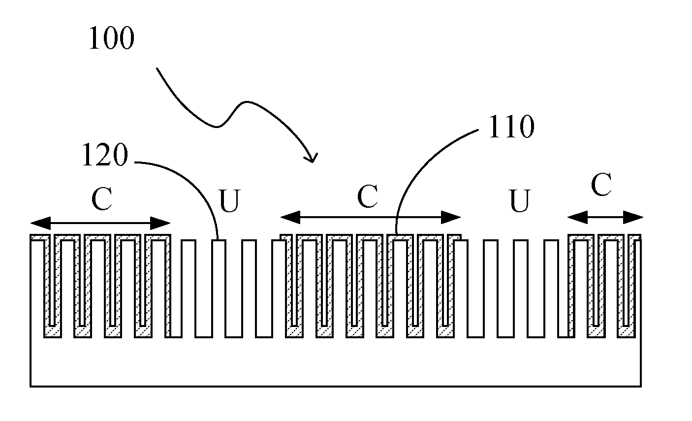
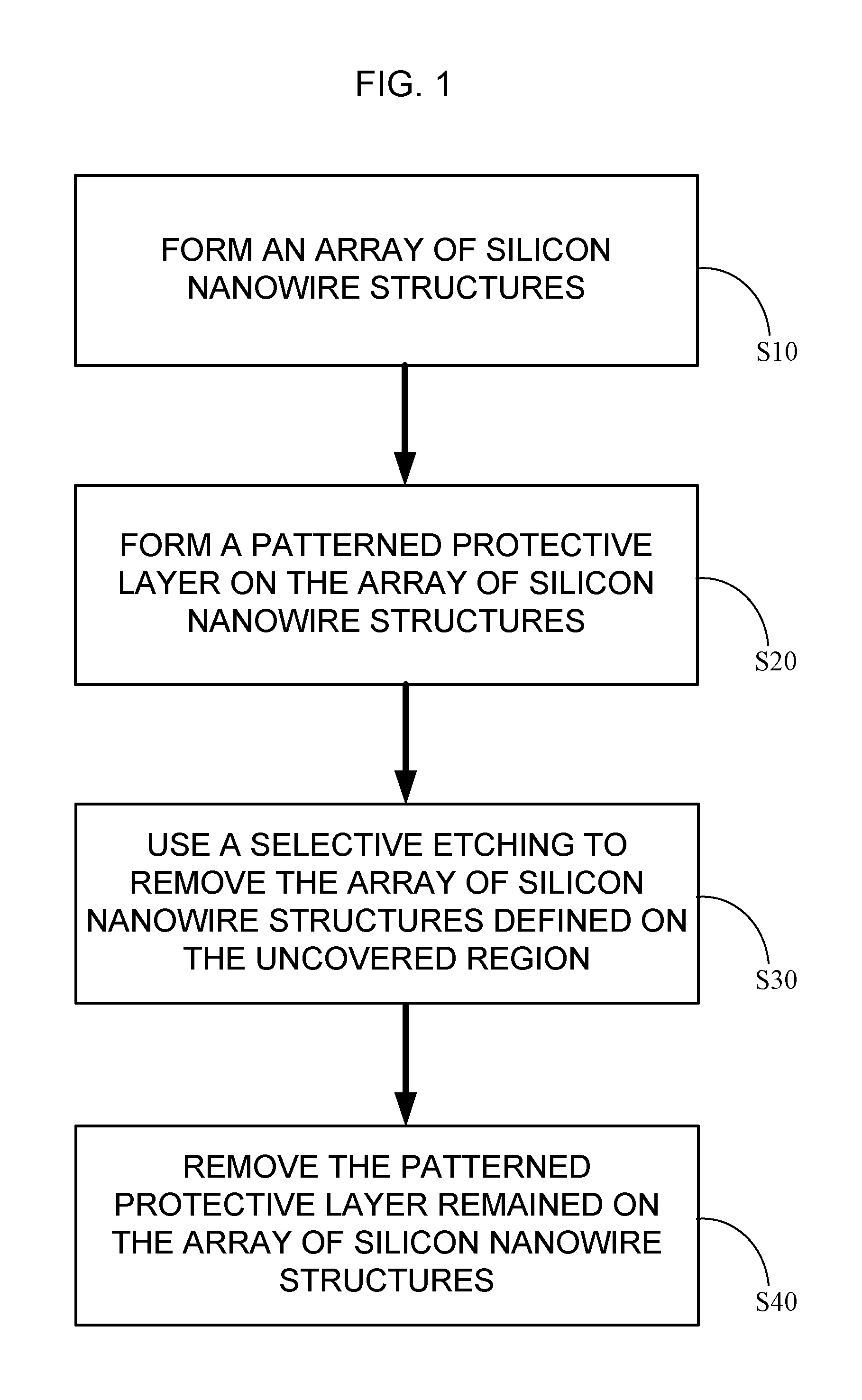
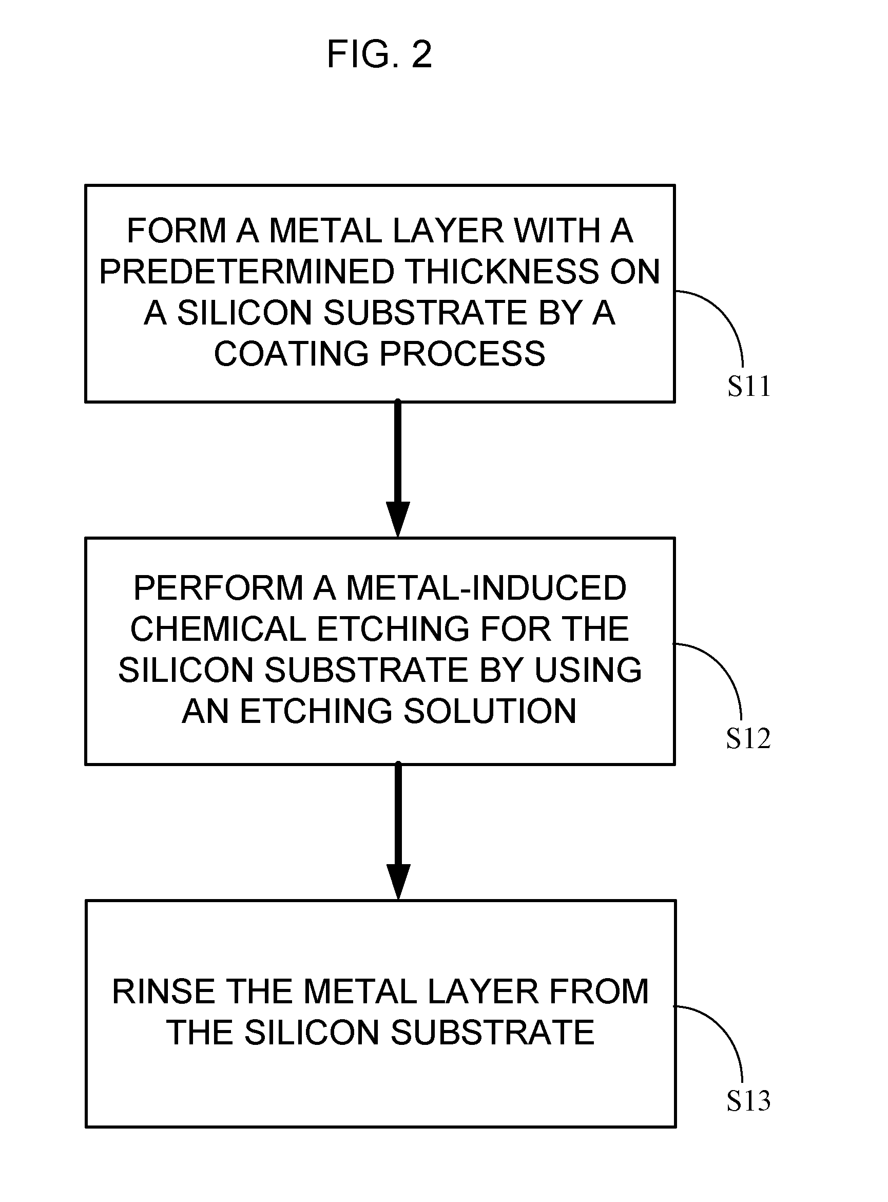
[0052]The following will explain a method for fabricating a patterned silicon nanowire array according to a preferred embodiment of the present invention in detail with drawings. Referring to FIG. 1 and FIG. 2, FIG. 1 is a flow chart illustrating a method for fabricating a patterned silicon nanowire array; FIG. 2 is a flow chart illustrating detailed steps of step S10. The fabrication method of the embodiment begins with step S10.

[0053]At step S10, silicon nanowire array structures are formed. As shown in FIG. 2, the step of forming the array of silicon nanowire structures begins with step S11. Referring to FIG. 3, FIG. 3 is a schematic section view illustrating a silicon substrate in performing step S11. Specifically, the array of silicon nanowire structures means the silicon nanowires with large area and uniform arrangement made on a silicon substrate 10. It should be noted that the silicon substrate 10 is a substrate which has a silicon layer on the surface thereof. The silicon m...


PUM

PropertyMeasurementUnit
thicknessaaaaaaaaaa
thicknessaaaaaaaaaa
thicknessaaaaaaaaaa

Abstract

A method for fabricating a patterned silicon nanowire array is disclosed. The method includes: forming a patterned protective layer on silicon nanowire array structures, forming a patterned protective layer on the array of silicon nanowire structures, the patterned protective layer defining a covered region and a uncovered region on the array of silicon nanowire structures; using a selective etching to remove the array of silicon nanowire structures defined on the uncovered region; and removing the patterned protective layer remained on the array of silicon nanowire structures. A method for fabricating a silicon microstructure is also disclosed.

Description

CROSS-REFERENCE[0001]This application claims the priority of Taiwan Patent Application No. 101127311, filed on Jul. 27, 2012. This invention is partly disclosed in papers: 1) “International Electron Devices and Materials Symposium (IEDMS), paper D4-4, Taiwan, Nov. 17-18, 2011,” entitled “Vertically-aligned silicon nanowire bundles for field emission applications” completed by Looi Choon Beng, Yung-Jr Hung, San-Liang Lee, Kuei-Yi Lee, Kai-Chung Wu, and Yen-Ting Pan. 2) “2012 the Conference on Lasers and Electro-Optics (CLEO), Paper CTh1C.5, San Jose, Calif., USA, May 6-11, 2012,” entitled “Top-down formation of vertically-aligned silicon nanowire bundles for tuning optical and field emission properties” completed by completed by Yung-Jr Hung, San-Liang Lee, Looi Choon Beng, Soo Chee Yeng, and Kuei-Yi Lee. 3) “Journal of Vacuum Science and Technology B, vol. 30, no. 3, pp. 030604-1˜030604-7, May / June 2012,” entitled “Formation of mesa-type vertically-aligned silicon nanowire bundle ar...

Claims


Application Information

Patent Timeline
Patent Type & Authority Applications(United States)
IPC IPC(8): H01L21/306H01L21/20
CPCB82Y40/00H01L29/16H01L21/20H01J1/304H01L31/035227H01J2201/3043H01L21/306H01L29/0676H01L21/30604B82Y10/00H01L21/3083H01L21/3081
Inventor HUNG, YUNG-JRLEE, SAN-LIANG
Owner NAT TAIWAN UNIV OF SCI & TECH
Why Eureka
Try Eureka