Method for fabricating two substrates connected by at least one mechanical and electrically conductive connection and structure obtained
- Summary
- Abstract
- Description
- Claims
- Application Information
AI Technical Summary
Benefits of technology
Problems solved by technology
Method used
Image

Examples
Embodiment Construction
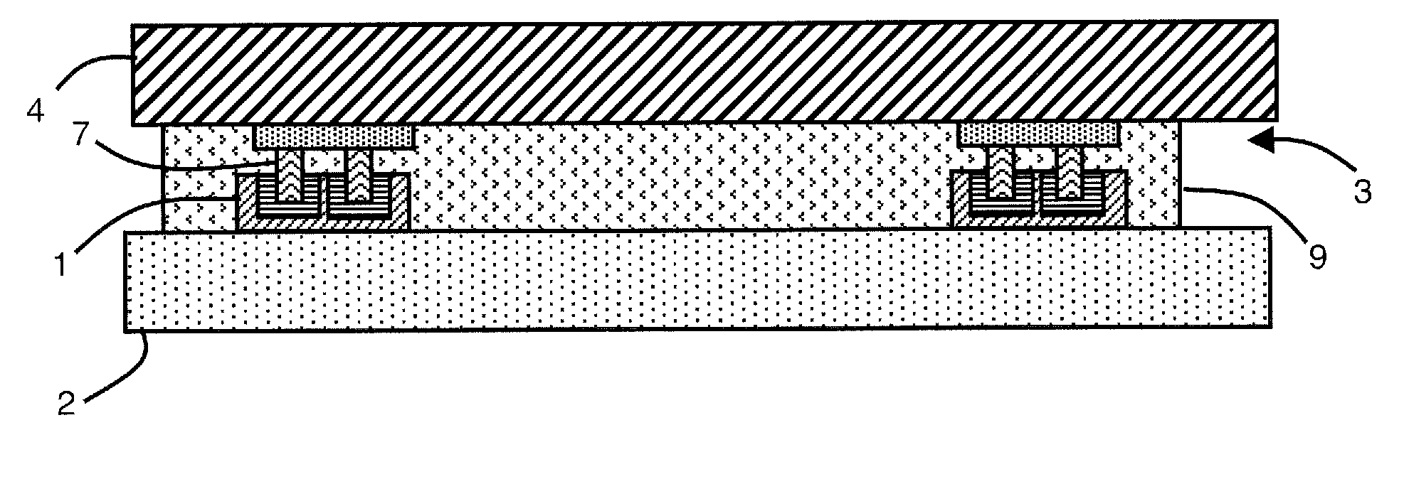
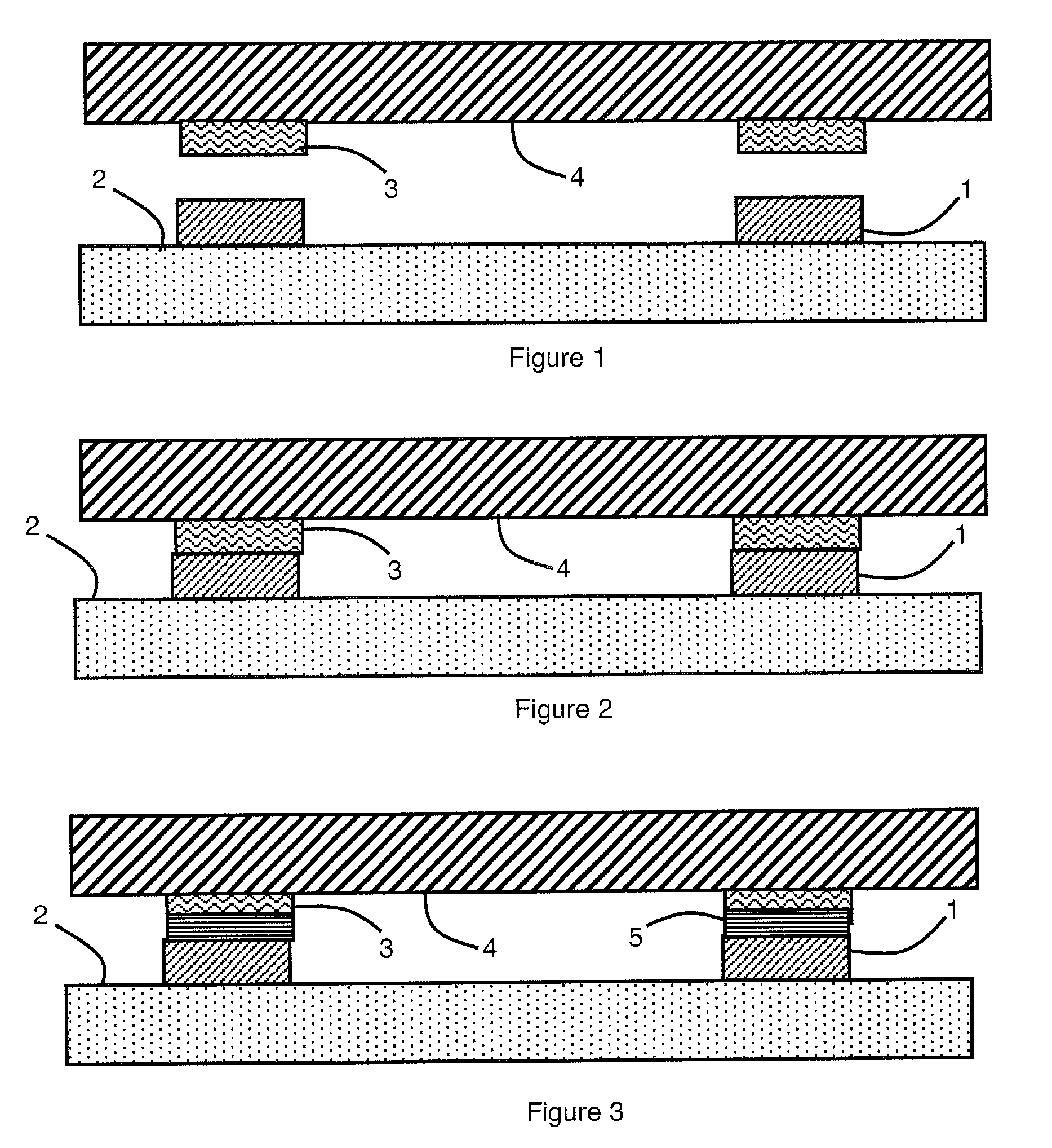
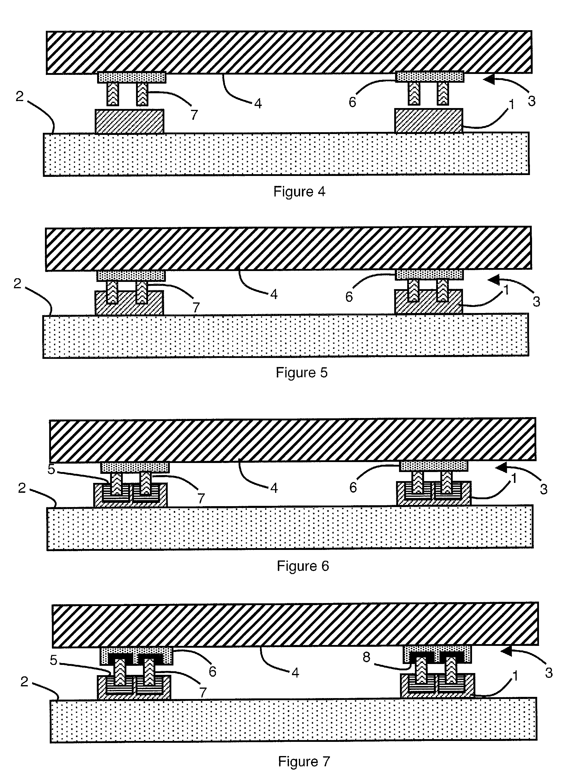
[0026]As illustrated in FIG. 4, a first substrate 2 comprises a main surface with an electric connection formed by a receiving area 1. Receiving area 1 is formed by a first metallic material. Receiving area 1 advantageously presents a flat free surface. However, in certain embodiments, the free surface can present a surface topography. The free surface is a surface that is uncovered or that can be covered by any material such as an oxide.
[0027]A second substrate 4 is used and it comprises a main surface with an electric connection formed by an insertion area 3. Insertion area 3 presents a surface topography which can be represented by a substantially flat base surface 6 at the surface of which a bump 7 is salient. Bump 7 is formed by a second metallic material. In certain embodiments, bump 7 and base surface 6 are formed from the second metallic material. In other embodiments, bump 7 and base surface 6 are formed from different materials. Bump 7 is secured to second substrate 4 by m...
PUM
| Property | Measurement | Unit |
|---|---|---|
| Pressure | aaaaa | aaaaa |
| Electrical conductivity | aaaaa | aaaaa |
| Ratio | aaaaa | aaaaa |
Abstract
Description
Claims
Application Information
 - R&D
- Intellectual Property
- Life Sciences
- Materials
- Tech Scout
- Unparalleled Data Quality
- Higher Quality Content
- 60% Fewer Hallucinations
Browse by: Latest US Patents, China's latest patents, Technical Efficacy Thesaurus, Application Domain, Technology Topic, Popular Technical Reports.
© 2025 PatSnap. All rights reserved.Legal|Privacy policy|Modern Slavery Act Transparency Statement|Sitemap|About US| Contact US: help@patsnap.com