
Anti-Reflection Film and Method for Manufacturing Anti-Reflection Film

a technology of anti-reflection film and anti-reflection film, which is applied in the direction of instruments, coatings, optics, etc., can solve the problems of poor anti-reflection performance, poor scratch resistance, and easy mechanical damage to the surface of the concave-convex nanostructure, so as to reduce the reflection of incident light, improve the anti-reflection film scratch resistance, and reduce the effect of incident light reflection

Active Publication Date: 2013-10-17
TAMRON
View PDF6 Cites 9 Cited by
  • Summary
  • Abstract
  • Description
  • Claims
  • Application Information

AI Technical Summary

Benefits of technology

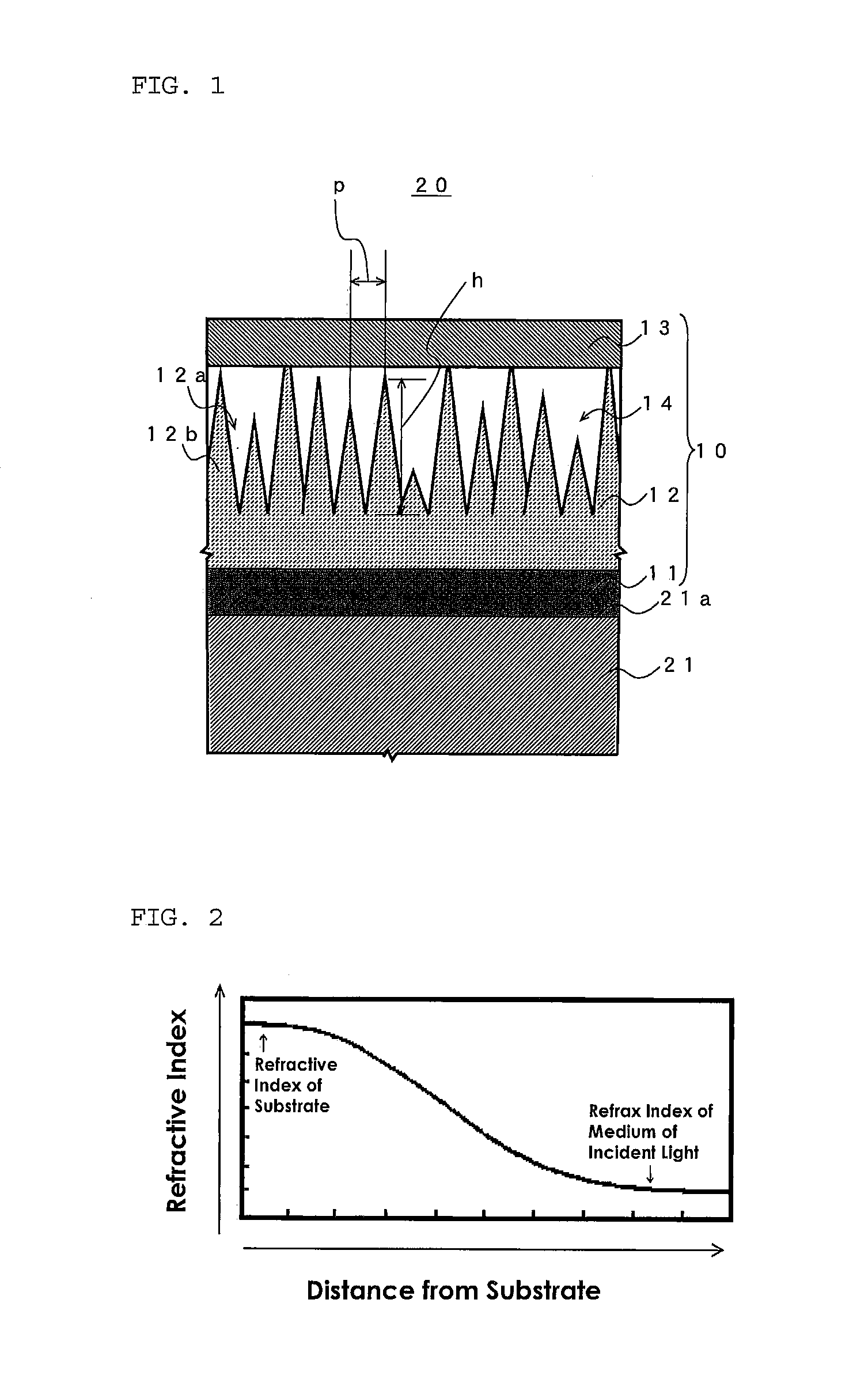
The present invention provides an anti-reflection film with improved resistance to high-temperature and high-humidity environments and scratches. This is achieved by providing a cover layer that prevents water or other substances from adsorbing onto the concave-convex nanostructure, which also prevents incident light from being reflected. Additionally, the anti-reflection film has a void between the cover layer and the concave parts of the nanostructure, which further reduces reflection. This combination of the cover layer and the base layer as optical thin films also makes the refractive index distribution in the film closer to an ideal, resulting in better anti-reflection performance. Overall, the present invention enhances the film's ability to prevent reflection and improve its durability.

Problems solved by technology

Thus, a problem that the surface of the concave-convex nanostructure might be easily damaged mechanically, i.e. poor in scratch resistance.
Thus, for example, when the concave-convex nanostructure is kept for a long period of time under a high-temperature and high-humidity environment, water or the like adsorbs to the concave-convex nanostructure and the spoiled concave-convex nanostructure may cause a problem, poor anti-reflection performance.
Thus, the gradual refractive index distribution formed in the depth direction of the concave-convex nanostructure from the air as the medium of incident light cannot be maintained, and the anti-reflection performance of the anti-reflection film may be made poor.
However, it is difficult to form the ideal refractive index distribution in the depth direction just by the concave-convex nanostructure, and further improvement in the anti-reflection performance is required.

Method used


Image

  • Anti-Reflection Film and Method for Manufacturing Anti-Reflection Film
  • Anti-Reflection Film and Method for Manufacturing Anti-Reflection Film
  • Anti-Reflection Film and Method for Manufacturing Anti-Reflection Film

Examples


example 2

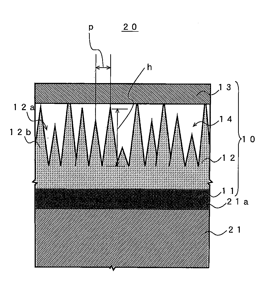
[0089]In Example 2, a glass lens made of N-BK7 glass (nd=1.52) manufactured by SCHOTT AG Corporation was used as the optical element 21. The concave-convex nanostructure 12 made of the PMMA resin was formed on the optical element 21. After that, SiO2 as the inorganic light-transmitting material was used as the raw material for deposition and the outer side of the concave-convex nanostructure 12 was covered with the cover layer 13 to manufacture the anti-reflection film 10 and the anti-reflection optical element 20 of Example 2. The steps of forming the respective layers will be more specifically described below.

[0090]First, a PMMA resin film was formed on the optical surface 21a by a spin coating method. The concave-convex nanostructure 12 was formed on the PMMA resin film in a similar method to Example 1. In the concave-convex nanostructure 12 formed in Example 2, the pitch width of the convex part 12b was about 100 nm to 200 nm, and the height h of the convex part 12b was about 12...

example 3

[0091]The anti-reflection film 10 and the anti-reflection optical element 20 of Example 3 were manufactured in a similar manner to the anti-reflection film 10 and the anti-reflection optical element 20 of Example 2 except that ZrO2+TiO2 was used as the inorganic light-transmitting material constituting the cover layer 13 and the film thickness of the cover layer 13 was 5 nm. The refractive index (nc) and the optical thickness (nc×dc) of the cover layer 13 were 1.8 and 9 nm respectively. The reference wavelength λ0 is 550 nm. Thus, the relationship in the expression (1) is satisfied.

example 4

[0092]In Example 4, a glass lens made of optical glass (product name: S-LAH55 (nd=1.83) manufactured by OHARA INC.) was used as the optical element 21. An optical thin film composed of a three-layer equivalent stack having a layer construction shown in Table 3 was formed as the base layer 11. Then, the concave-convex nanostructure 12 made of the PMMA resin was formed on the base layer 11. After that, MgF2 as the inorganic light-transmitting material was used as the raw material for deposition and the outer side of the concave-convex nanostructure 12 was covered with the cover layer 13 to manufacture the anti-reflection film 10 and the anti-reflection optical element 20 of Example 4. The steps for forming the respective layers will be more specifically described below.

[0093]First, the method for forming the base layer 11 will be described. An Al2O3 film was deposited as a first layer on the optical surface 21a of the glass lens so as to have a physical thickness of 29.4 nm by the vac...


PUM

PropertyMeasurementUnit
refractive index ncaaaaaaaaaa
refractive indexaaaaaaaaaa

Abstract

An object of the present invention is to provide an anti-reflection film excellent in high-temperature and high-humidity environment resistance and scratch resistance in addition to improved anti-reflection performance of a concave-convex nanostructure. To achieve the object, an anti-reflection film 10 comprises: a base layer 11 as a first optical thin film that is provided on an optical surface 21a of an optical element 21; a concave-convex nanostructure layer that is provided on a surface of the base layer 11 and is composed of a concave-convex nanostructure 12 formed so as to have a pitch width p between the convex parts 12b of shorter than an incident light wavelength; and a cover layer 13 as a second optical thin film that covers peaks of the convex part 12b with a void 14 being provided between the cover layer 13 and concave part 12a constituting the concave-convex nanostructure 12.

Description

BACKGROUND OF THE INVENTION[0001]1. Field of the Invention[0002]The present invention relates to an anti-reflection film which is provided on an optical surface of an optical element main-body to reduce reflection of incident light, and a method for manufacturing the anti-reflection film and more particularly relates to an anti-reflection film comprising a concave-convex nanostructure, and a method for manufacturing the anti-reflection film.[0003]2. Background Art[0004]In a conventional optical element such as a lens, an anti-reflection film comprising an anti-reflection structural body is provided on an optical surface to reduce a loss of transmitting light due to surface reflection. A concave-convex nanostructure in which convex parts are regularly arranged at a shorter interval than the wavelength of incident light has been known as one example of the anti-reflection structural body (e.g., see “Patent document 1: National Publication of International Patent Application No. 2010-5...

Claims


Application Information

Patent Timeline
Patent Type & Authority Applications(United States)
IPC IPC(8): G02B1/11B32B7/02G02B1/02G02B1/118G02B5/02
CPCG02B1/11G02B1/118G02B1/115
Inventor MIYAHARA, MASAAKISHIBUYA, MINORUKUNISADA, TERUFUSA
Owner TAMRON
Learn More