
Pixel circuit and driving method thereof

a technology of pixel circuit and driving method, which is applied in the field of pixel circuit, can solve the problems of increasing power consumption, high parasitic capacitance, and tending to occur variations in electric characteristics, and achieves the effect of reducing power consumption, high resolution, and correcting the variation of threshold voltage of driving transistor

Active Publication Date: 2013-08-29
CANON KK
View PDF7 Cites 15 Cited by
  • Summary
  • Abstract
  • Description
  • Claims
  • Application Information

AI Technical Summary

Benefits of technology

The present invention provides a pixel circuit and a driving method that can correct variations in the threshold voltage of a driving transistor, reduce power consumption, and achieve high resolution. The invention automatically adjusts the gate-source potential difference of the driving transistor to the threshold voltage, which eliminates the necessity for a power source line control switch and multiple capacitors. This reduces power consumption and voltage withstanding load to the transistor, increasing reliability and allowing for high resolution.

Problems solved by technology

However, the transistor Tr formed of polysilicon has a problem in that variation in electric characteristics tends to occur owing to lattice defect on crystalline grain boundaries.
However, in the case of driving by changing the potential of the power source line, the power source line typically has a wide wiring width to reduce the resistance and thus has a high parasitic capacitance.
Accordingly, there is a problem in that change in potential of the power source line increases power consumption.
At the same time, a switch for changing the potential of the power source line is arranged, which causes a problem in that it is difficult to achieve high resolution.
Accordingly, there is a problem in that the required voltage range is increased and thus power consumption is increased.
However, requirement of the plurality of capacitors in the pixel circuit causes a problem in that it is difficult to achieve high resolution.

Method used


Image

  • Pixel circuit and driving method thereof
  • Pixel circuit and driving method thereof
  • Pixel circuit and driving method thereof

Examples


first embodiment

[0023]An example of an organic EL display apparatus to which a pixel circuit of the present invention is applied will now be described as a first embodiment.

[0024]1. Pixel Circuit Configuration

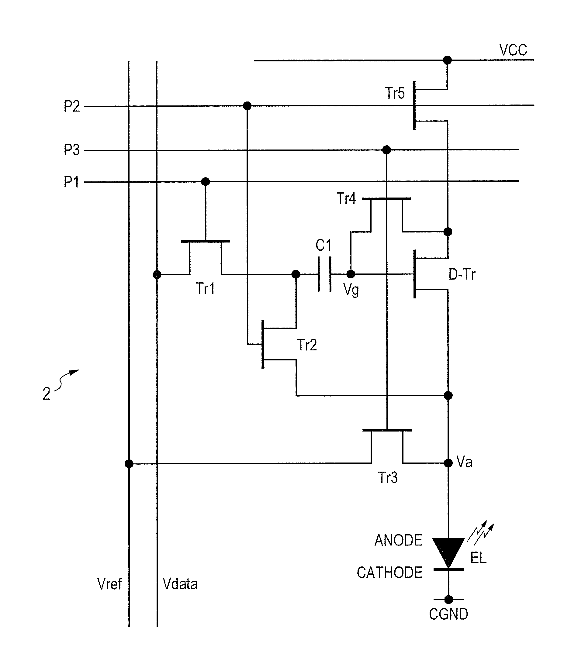
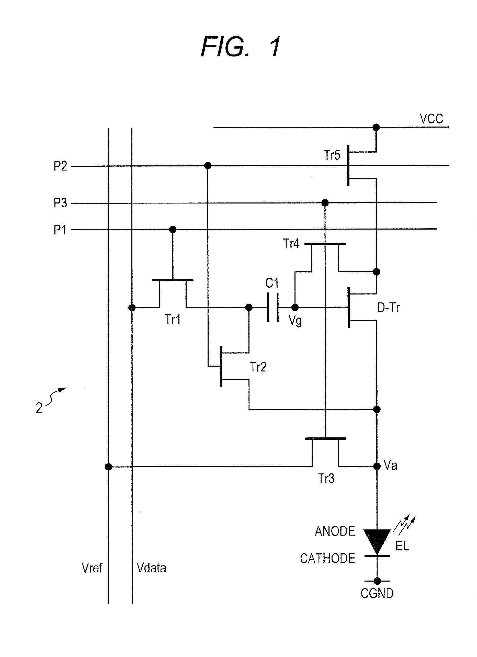
[0025]FIG. 1 is an example of a pixel circuit 2. A first switching transistor Tr1 functions as a switch connecting a capacitor C1 to a data line. The transistor Tr1 is an N-channel transistor. The gate electrode is connected to a P1 control signal line. This transistor is conduct during the control signal P1 being at an “H” (HIGH) level, and captures a data voltage Vdata of the data line into the pixel circuit 2. One end of the capacitor C1 is connected to the gate electrode of a driving transistor (D-Tr) controlling a rate of current flowing to a light emitting element. The other end of the capacitor C1 is connected to the transistor Tr1. The anode electrode of the light emitting element is connected to the source electrode of the D-Tr, and the cathode electrode is connected to a constant pot...

second embodiment

[0058]1. Pixel Circuit Configuration

[0059]FIG. 4 is a variational example of the pixel circuit of FIG. 1. The connection relationship of the transistors and capacitor elements in the pixel circuit are the same as those in the first embodiment. The transistors Tr3 and Tr4 are not connected to the P3 control signal line on the i-th row but are connected to the P1 control signal line on the (i−1)-th row (row preceding) instead, which is different from that of the first embodiment.

[0060]2. Display Apparatus Configuration

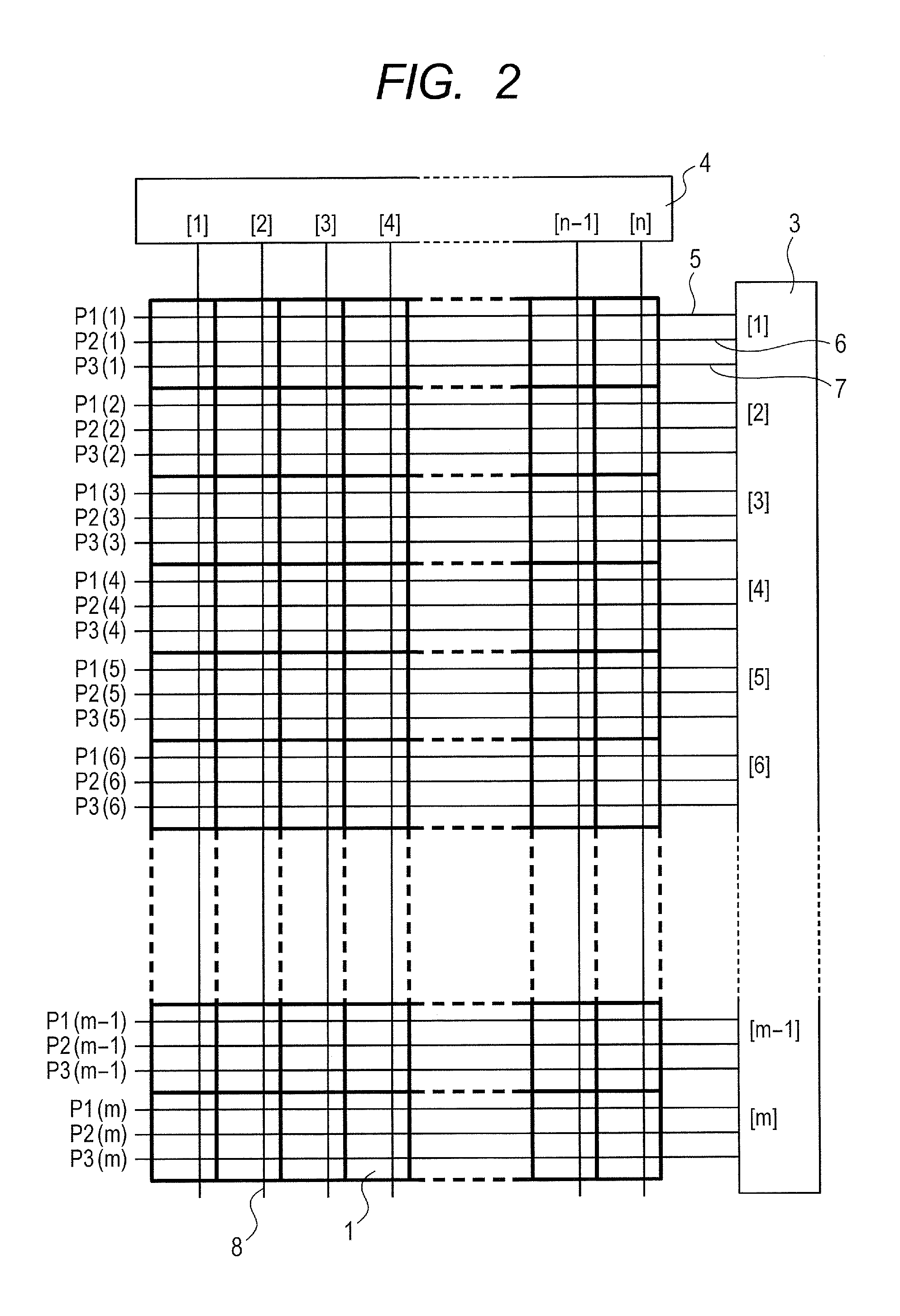
[0061]Two control signal lines, instead of three, extend from the row controlling circuit 3 on each row, which are different from those of the first embodiment. The control signals P1(1) to P1(m), and P2(1) to P2(m) on the total m rows are output to the control signal line, and the control signal P1(i−1) on the row preceding in addition to the control signal on the row operated is input into the pixel circuit 2, which are different from those of the first embodiment. Oth...

third embodiment

[0065]1. Pixel Circuit Configuration

[0066]FIG. 6 is a variational example of the pixel circuit of FIG. 4. The connection relationship between the transistors and capacitor elements in the pixel circuit is the same as that of the second embodiment. The one end of the transistor Tr3 is not connected to the reference voltage line but is connected to the P2 control signal line on the (i−1)-th (row preceding), which is different from that of the second embodiment. During time in which the transistor Tr3 is ON, that is, a period in which P1(i−1) is “H”, connection to the control signal line being at “L” inputs the low level of the control signal line as voltage Vref into the pixel. Accordingly, in addition to FIG. 6, connection to the P1 control signal line on the (i+1)-th row (row following thereto) instead of the P2 control signal line on the (i−1)-th row (row preceding) can also exert the analogous effects.

[0067]2. Display Apparatus Configuration

[0068]The control signal P2(i−1) on the ...


PUM


Abstract

A pixel circuit with a source follower type connection is provided that corrects variation in threshold voltage of a driving transistor, reduces power consumption and realizes high resolution. The pixel circuit includes: a data line for supplying a data voltage; a power source line for supplying a power source voltage; a reference voltage line for supplying a reference voltage lower than the power source voltage; a plurality of control signal lines for supplying control signals; a light emitting element; a driving transistor; a capacitor; and a plurality of switching transistors. The circuit writes the data voltage through one end of the capacitor and subsequently connects the one end of the capacitor to the anode electrode of the light emitting element.

Description

BACKGROUND OF THE INVENTION[0001]1. Field of the Invention[0002]The present invention relates to a pixel circuit including a light emitting element and a driving method thereof and, in particular, to a pixel circuit applicable to a display apparatus of a self-light-emitting type and a driving method thereof.[0003]2. Description of the Related Art[0004]An display apparatus of the self-light-emitting type, which is typified by an organic electroluminescence (EL) display apparatus, is configured by arranging a plurality of pixels in a matrix on a substrate. In each pixel, a pixel circuit including a light emitting element is arranged. To cause the light emitting element of each pixel to emit light with a luminance based on an image data of each pixel, a current rate flowing into each light emitting element is required to be accurately controlled. Typically, a display apparatus of the self-light-emitting type has an active matrix configuration where an active element (which hereinafter ...

Claims


Application Information

Patent Timeline
Patent Type & Authority Applications(United States)
IPC IPC(8): G09G3/32H05B33/08H05B44/00
CPCG09G3/3233H05B33/08G09G3/3258G09G2300/0861H05B44/00
Inventor IKEDA, KOUJI
Owner CANON KK
Learn More