Optical conversion element and optical conversion element manufacturing method

a manufacturing method and optical conversion technology, applied in the field of optical conversion elements and optical conversion elements manufacturing methods, can solve the problems of reducing optical coupling efficiency, difficult adiabatic change in mode field, and inability so as to improve device and system performance including optical circuits, and achieve high optical coupling efficiency.

Inactive Publication Date: 2013-07-25
NEC CORP
View PDF6 Cites 19 Cited by
  • Summary
  • Abstract
  • Description
  • Claims
  • Application Information

AI Technical Summary

Benefits of technology

The present invention improves the coupling between an optical circuit and an optical fiber on a substrate, leading to better performance of the device and system. It is easy to achieve high coupling efficiency, making the connection process easier and more productive. Additionally, it does not require anti-reflective coating for each chipped waveguide end, increasing productivity.

Problems solved by technology

Although a small core size and mold field size are advantageous to integration of optical circuits, they pose a problem in optical coupling with an external optical system.
Although the mode field usually indicates distribution of an electric field, high optical coupling efficiency cannot be achieved unless distribution of magnetic field is conformed at the same time.
When the effective refractive indices are not conformed, light is reflected at an interface between the connected two waveguides, thereby reducing the optical coupling efficiency.
An issue in the spot size converter according to the first technique is that the larger a difference in the sizes of the first core and the second core, the more difficult an adiabatic change in the mode field would be.
However, in practice, the greater the ratio of the mode field expanded outside the first core, the larger the ratio of the change in the mode field size to the change in the size of the first core, thereby making a gradual change in the mode field size difficult.
Consequently, the size of the mode field that can adiabatically change is limited.
Therefore, even when there is a large difference in the cross-sectional size of the core before and after the conversion, limitation in manufacture as in the first technique would not be generated.
Although the spot size converter by the second technique includes a gradual vertical taper, a formation technique of such vertical taper cannot be used in some cases.
However, the second and third techniques have a common issue.
The issue is that the effective refractive index of the guided light cannot be largely changed as the refractive indices of the material forming the first and second cores are almost the same.
Meanwhile, the effective refractive index of guided light in general optical fibers for communication is about 1.5, and simply connecting the spot size converter to this optical fiber will reduce the optical coupling efficiency clue to interface reflection.
Anti-reflective coating on an endface of the waveguide of the optical circuit suppresses the reflection but it is not suitable for high-volume manufacturing.
The same problem arises when the anti-reflective coating is applied on the side of optical fibers instead of the optical circuit chips.
As stated above, the spot size converters according to the first to third techniques have issues including the limitation of the maximum expandable size of the mode field and necessity of anti-refractive coating.

Method used


Image

  • Optical conversion element and optical conversion element manufacturing method
  • Optical conversion element and optical conversion element manufacturing method
  • Optical conversion element and optical conversion element manufacturing method

Examples


first exemplary embodiment

(Modification of First Exemplary Embodiment)

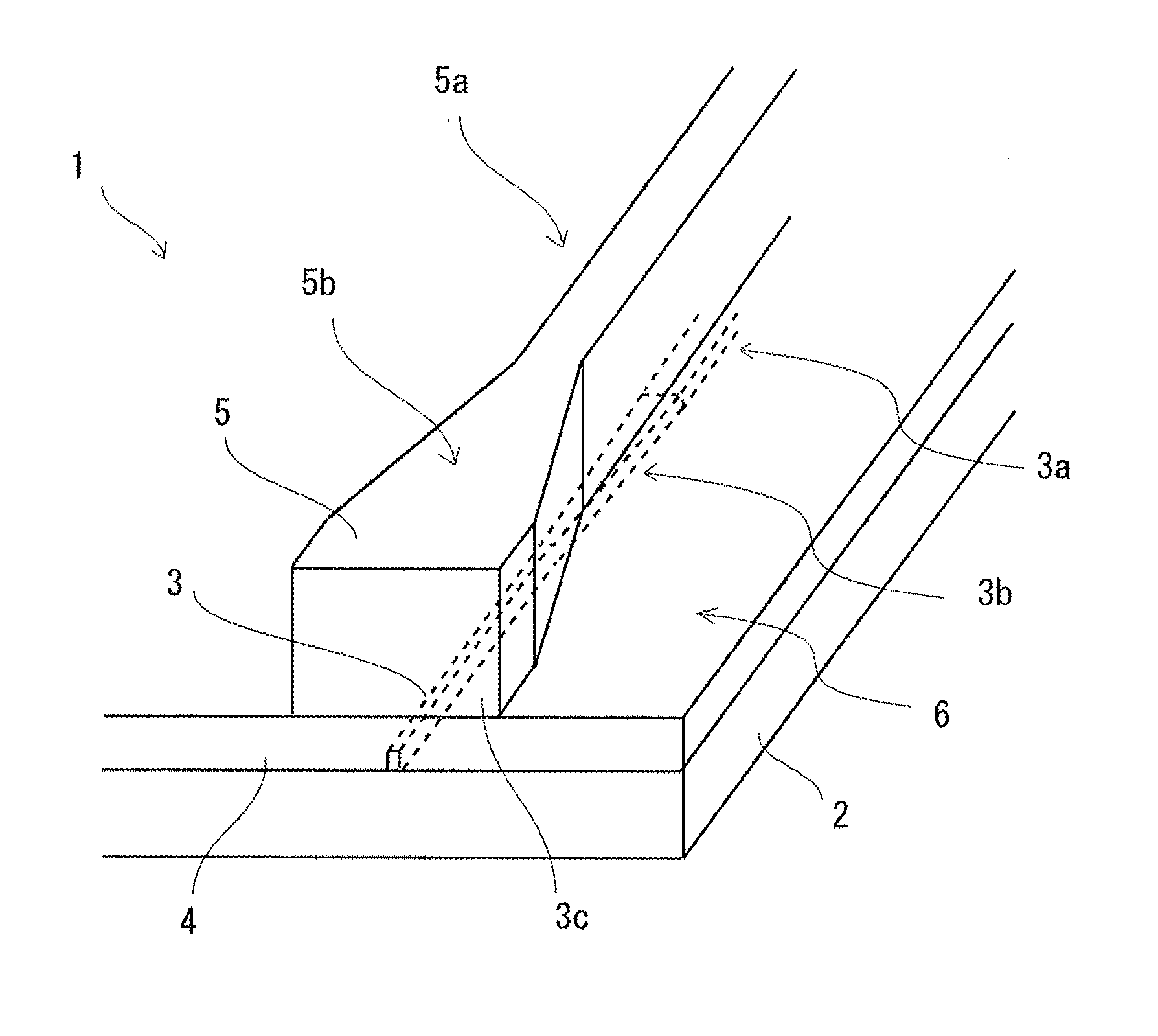
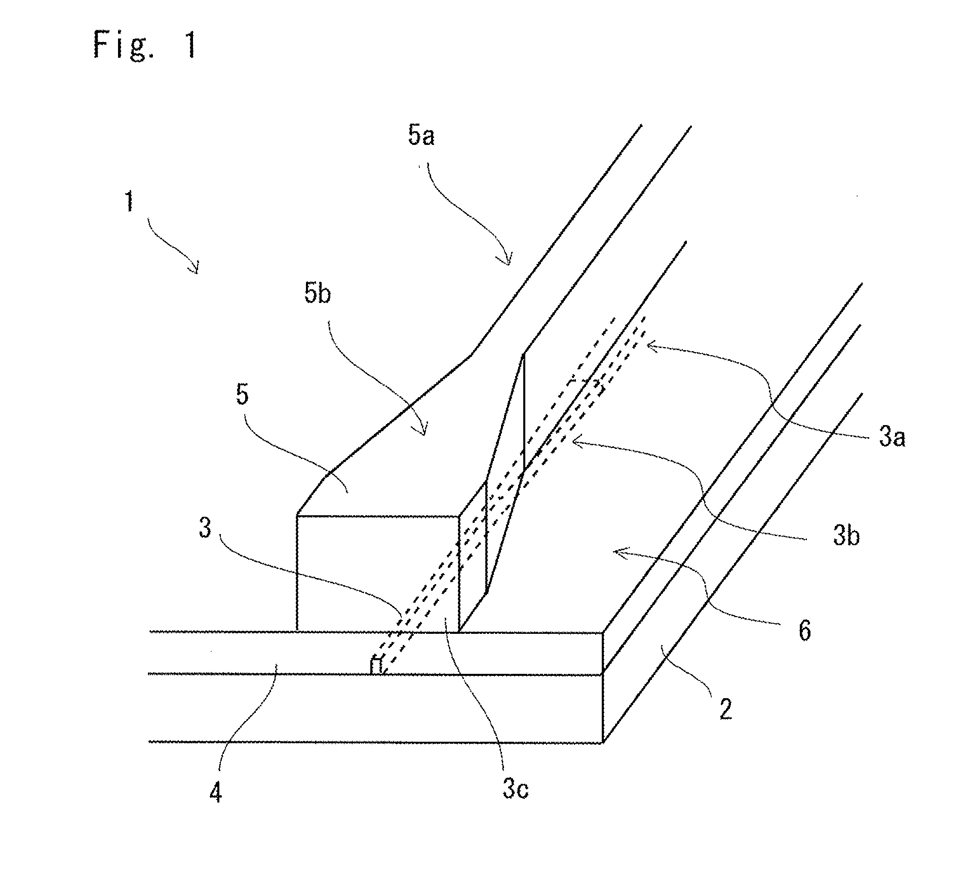
[0114]There is no big change in the operation with the structure including slight modification from the first exemplary embodiment. That is explained with reference to FIG. 4. Both FIGS. 4A and 4B are cross-sectional diagrams showing modified structures of the optical conversion element according to the first exemplary embodiment of the present invention.

[0115]FIG. 4A shows a cross-section of a tapered part 51b of the ridge 5 in the second tapered part 1b (see FIG. 2A) as a modification. As in this modification shown in FIG. 4A, the cross-section of the ridge 5 is not a rectangular but may alone have a convex cross-section structure with thin films on both sides of a bottom part. As described above, FIG. 4A shows the cross-section of the tapered part 51b of the ridge 5 in the second tapered part 1b, and the narrow width part 5a of the ridge 5 in the first tapered part 1a (see FIG. 2A) may also have a convex cross-sectional structure in a s...

second exemplary embodiment

[0118]Next, a second exemplary embodiment of the optical conversion element according to the present invention is explained with reference to the drawings.

[0119]FIG. 5A is a top view of the optical conversion element according to the second exemplary embodiment of the present invention. FIG. SB is a cross-sectional diagram taken along the line VB-VB of FIG. 5A.

[0120]As for an optical conversion element 13 according to the second exemplary embodiment, although the structure of the first outer core (slab 43 and ridge 53) is almost the same as that of the first exemplary embodiment, the structures of the inner cores are different. As shown in FIG. 5A, in a range of a first tapered part 13a, a thin wire core 33 includes a large cross-sectional area part 33a, which is the same core as the waveguide of the optical circuit and has the largest cross-sectional area, and a tapered part 33b with its cross-sectional area decreasing from the optical circuit side to the optical fiber side. Furthe...

example 1

[0124]The present invention is explained in more detail based on an example 1. The specific structure of the optical conversion element according to the present invention was examined by calculation on how the mode field changes. The calculation of the mode field was performed by the finite element method.

[0125]As the example 1, a structure was analyzed in which the optical conversion element 1 according to the first exemplary embodiment was created in an optical circuit on an SOI substrate. Structural parameters were that the refractive index of the material forming the lower cladding 2 was 1.452 and the thickness thereof was 3.00 μm, the refractive index of the material forming the thin wire core 3 was 3.480, the refractive index of the material forming the slab layer 4 was 1.496 and the thickness thereof was 2.00 μm, the refractive index of the material forming the ridge 5 was 1.496 and the thickness thereof was 9.5 μm, and the refractive index of the material forming the top cla...


PUM


Abstract

Disclosed is an optical conversion element capable of highly efficient optical coupling between a silicon waveguide and a general single-mode optical fiber only by butt-coupling without requiring anti-reflective coating. One embodiment is an optical conversion element that includes a waveguide structure and converts a mode field of guided light and is characterized in that at least a dual core is included, an innermost core of the dual core is a silicon inverse tapered thin wire core, a first outer core is a forward tapered ridge core having a ridge structure formed of an oxide film with only width of the ridge core changing. The first outer core is positioned on a narrow width side of the innermost core.

Description

TECHNICAL FIELD[0001]The present invention relates to an optical conversion element and an optical conversion element manufacturing method, and particularly to an optical conversion element and an optical conversion element manufacturing method for realizing highly efficient optical coupling between a thin wire waveguide including a medium with a high refractive index such as silicon as a core and a single-mode optical fiber for optical communication.BACKGROUND ART[0002]An optical waveguide with its core being formed of a medium with a high refractive index such as silicon barely generates an optical loss even in the case of a sudden bend, thereby making it suitable for integration of optical circuits. One of optical waveguides attracting attention is an optical waveguide using a Silicon-on-Insulator (SOI) substrate.[0003]The SOI substrate is composed of a silicon base substrate, a Buried Oxide (BOX) layer thereon, and a silicon layer (SOI layer) on the BOX layer. With the SOI subst...

Claims


Application Information

Patent Timeline
IPC IPC(8): G02B6/26B29D11/00
CPCG02B6/1228G02B6/268B29D11/00663G02B6/305
Inventor TOKUSHIMA, MASATOSHINAKAMURA, SHIGERU
Owner NEC CORP
Why Eureka
Try Eureka