Shift Register and Gate Driving Circuit Using the Same
a technology of shift register and gate driving circuit, which is applied in the direction of digital storage, instruments, computing, etc., can solve the problems of exacerbated foregoing problems, display having a bigger size, and conventional shift register, and achieve excellent reliability
- Summary
- Abstract
- Description
- Claims
- Application Information
AI Technical Summary
Benefits of technology
Problems solved by technology
Method used
Image
Examples
first exemplary embodiment
(1) Configuration
[0094]As shown in FIG. 5, the shift register according to the first exemplary is embodiment includes eight switching devices TFT: T1˜T8 as follows.
[0095]The first switching device T1 has a gate terminal connected to an output terminal of the previous shift register N−2 or N−1, a drain terminal to receive the forward input signal FW, and a source terminal connected to the P node. The forward input signal has a VGH in the case of the forward driving and a VGL in the case of the backward driving.
[0096]The second switching device T2 has a gate connected to an output terminal of the subsequent shift register N+2 or N+1, a drain terminal to receive a backward input signal, and a source terminal connected to the P node. The backward input signal has a VGL in the case of the forward driving and a VGH in the case of the backward driving.
[0097]The third switching device T3 has a gate terminal to receive the control clock signal CLK3 or CLK1 through the capacitor, a drain term...
second exemplary embodiment
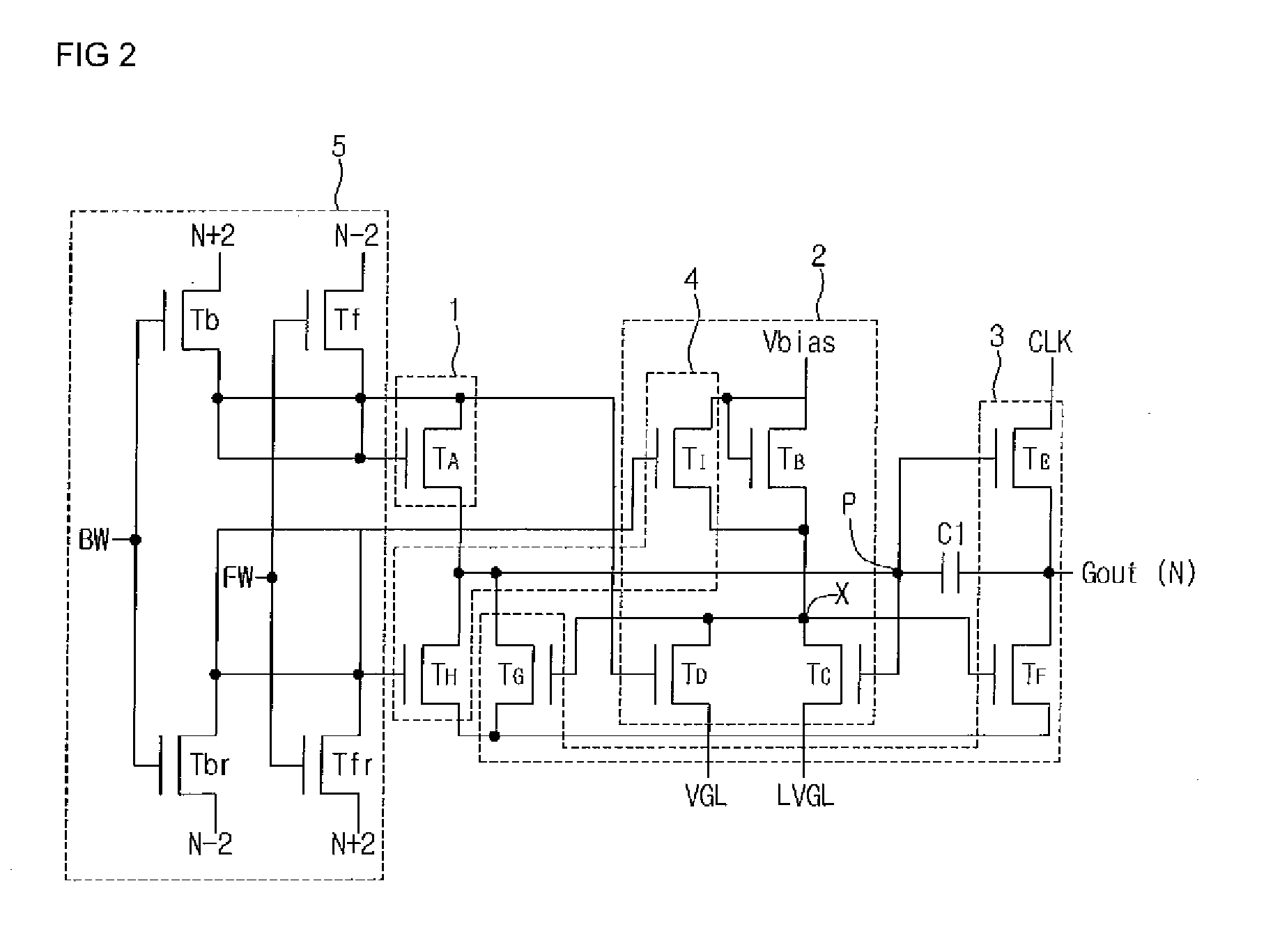
[0124]FIG. 8 illustrates a detailed circuit diagram of a shift register according to a second exemplary embodiment of the invention.
[0125]The second exemplary embodiment shows the same configurations as the input unit 10 and the output unit 30 of the first exemplary embodiment, but is different in an inverter unit. That is, on the contrary to the inverter unit 20 of the first exemplary embodiment of the invention, an inverter unit 21 of the second exemplary embodiment of the invention inputs a high level voltage signal VBIAS (a bias voltage signal) instead of the control clock signal CLK3 to the drain terminal of the device T3.
[0126]In the first exemplary embodiment, a high voltage at the X node always has a voltage VGH. On the other hand, in the second exemplary embodiment, the high voltage at the X node can be adjusted by a bias voltage, and thus it is possible to reduce stress applied to the devices T7 and T8.
[0127]The second exemplary embodiment has the same operation as the fir...
third exemplary embodiment
[0128]FIG. 10 is a detailed circuit diagram of a shift register according to a third exemplary embodiment of the invention.
[0129]The third exemplary embodiment further includes a stabilizer 40 for increasing the voltage at the X node by the gate start pulse (STP), compared with the second exemplary embodiment.
[0130]For example, the stabilizer 40 may be configured by a switching device T9 that has a gate terminal to receive the gate start pulse, a drain terminal to receive the bias voltage signal, and a source terminal connected to the X node.
[0131]The stabilizer 40 makes each shift register have a high-level voltage at the X node at the initial driving as shown in the timing diagram of FIG. 11 and turn on the devices T7 and T8. Thus, the voltages at the P node and the output terminal are stabilized into a base voltage state, and it is therefore possible to close off probability of abnormal driving at the first frame.
[0132]However, the STP signal supplied to the stabilizer 40 is not ...
PUM
 Abstract
Description
Claims
Application Information
 - R&D Engineer
- R&D Manager
- IP Professional
- Industry Leading Data Capabilities
- Powerful AI technology
- Patent DNA Extraction
Browse by: Latest US Patents, China's latest patents, Technical Efficacy Thesaurus, Application Domain, Technology Topic, Popular Technical Reports.
© 2024 PatSnap. All rights reserved.Legal|Privacy policy|Modern Slavery Act Transparency Statement|Sitemap|About US| Contact US: help@patsnap.com


