
Bulk Growth Grain Controlled Directional Solidification Device and Method

a technology of directional solidification and bulk growth, which is applied in the direction of crystal growth process, polycrystalline material growth, chemistry apparatus and processes, etc., can solve the problems of time-consuming and expensive single crystal si production, and achieve the effect of reducing heat loss

Inactive Publication Date: 2013-06-20
SPX CORP
View PDF3 Cites 21 Cited by
  • Summary
  • Abstract
  • Description
  • Claims
  • Application Information

AI Technical Summary

Benefits of technology

The present invention is a solidification system that helps improve the process of making silicon crystals. This results in higher quality silicon crystals.

Problems solved by technology

Unfortunately, single-crystal Si is expensive and time consuming to produce.

Method used


Image

  • Bulk Growth Grain Controlled Directional Solidification Device and Method
  • Bulk Growth Grain Controlled Directional Solidification Device and Method
  • Bulk Growth Grain Controlled Directional Solidification Device and Method

Examples


Embodiment Construction

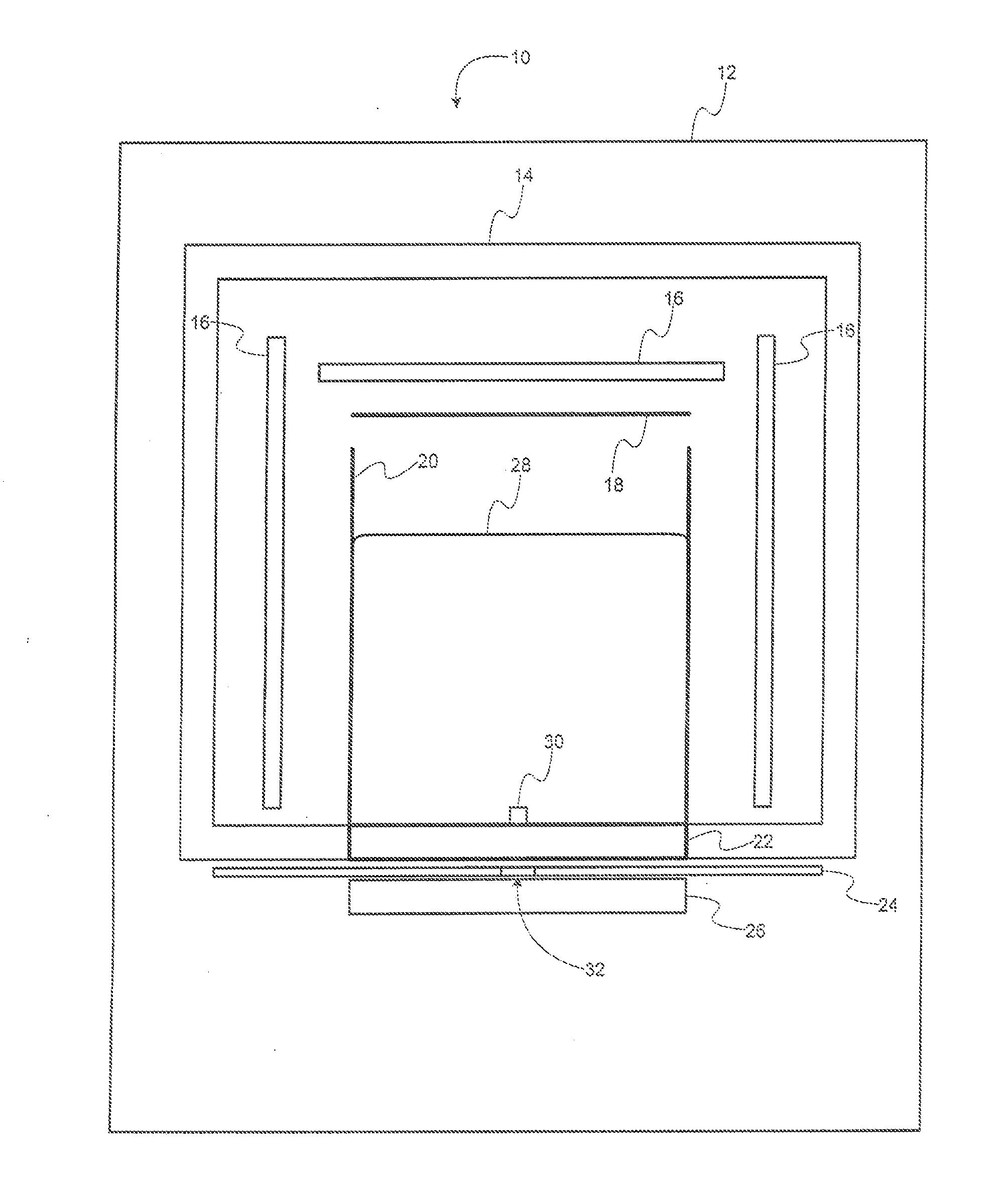
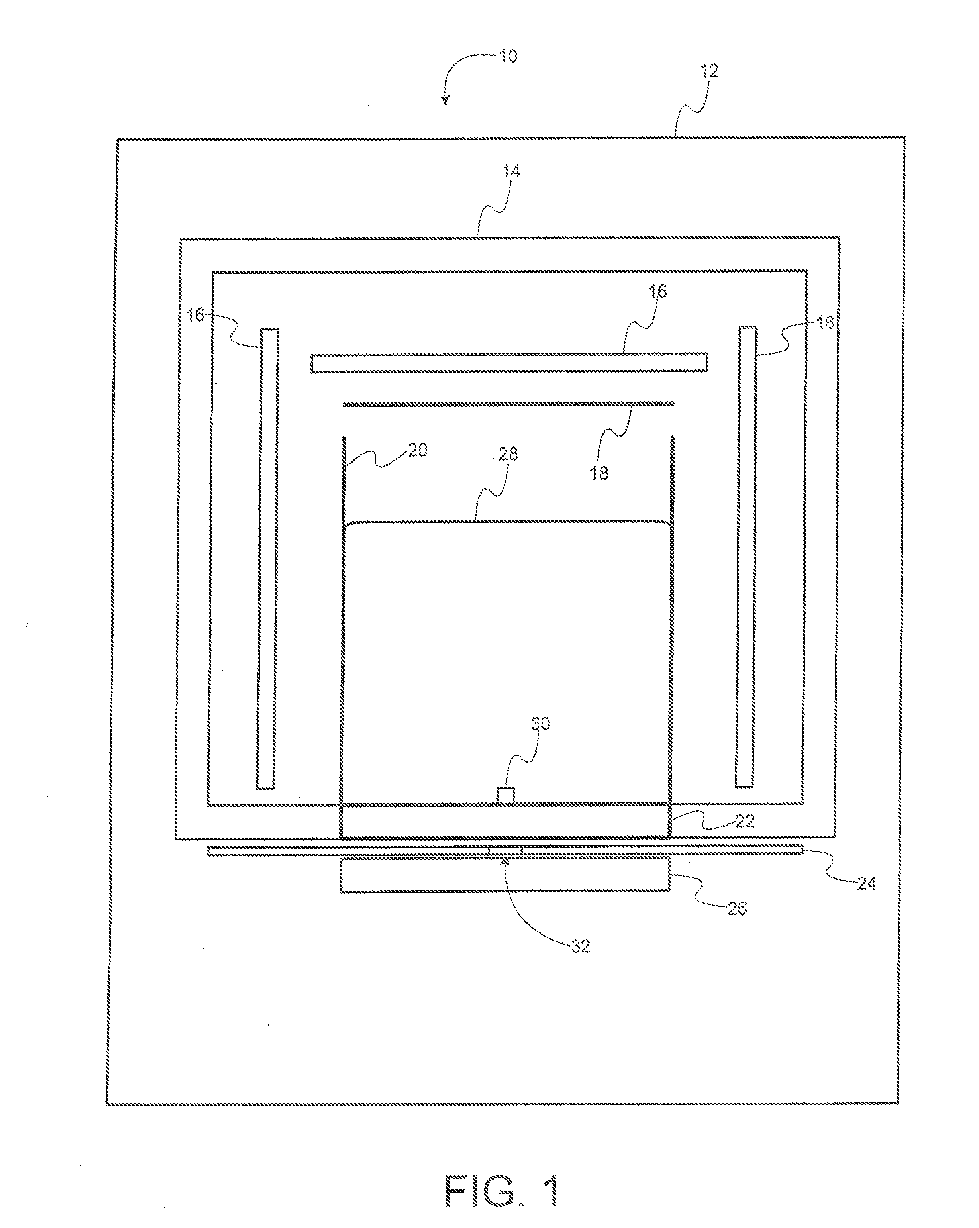
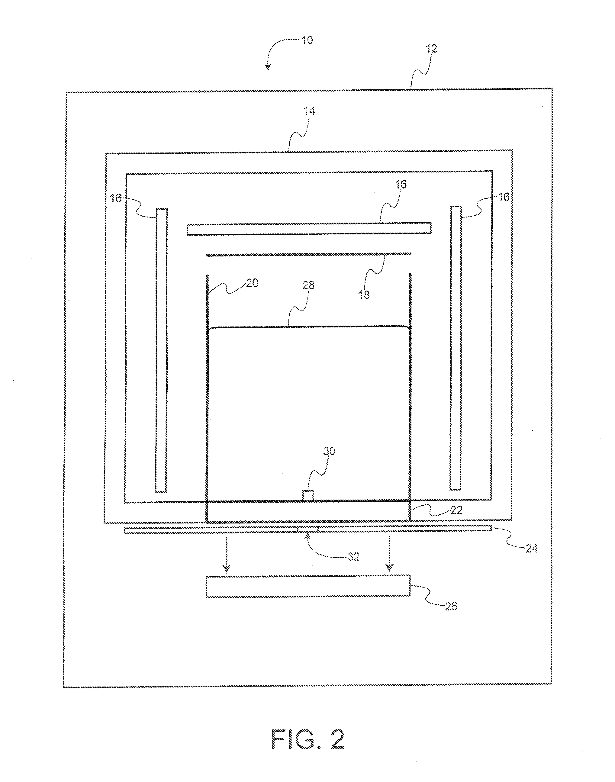
[0025]The present invention provides a mono-crystalline silicon (Si) directional solidification technology that starts with a relatively smaller size seed as compared to conventional solidification technologies. In some embodiments, a directional solidification casting system and a corresponding process are provided. The Si ingot produced by this technique possesses mono-crystalline microstructure with low impurities and long minority-carrier life, which gives rise to an equivalent cell efficiency as mono-crystalline Si manufactured via conventional Czochralski (CZ) process.

[0026]Embodiments of this invention provide an accurate control of the thermal conditions affecting crystal nucleation behavior and growth direction / grain size to enhance the silicon ingot quality produced by an industrial directional solidification growth. A variable heat control system allows for adjusting the heat flow through the bottom of the crucible during the solidification. The thermal conditions may be ...


PUM

PropertyMeasurementUnit
volumeaaaaaaaaaa
heat lossaaaaaaaaaa
radiant heat lossaaaaaaaaaa

Abstract

A solidification system is provided and includes a crucible, heater, insulation, movable insulation, and radiation regulator. The crucible is configured to retain a volume of silicon. The heater is to heat the crucible. The heater being configured to provide sufficient heat to melt the volume of silicon. The insulation is to reduce heat loss from a first portion of the crucible. The movable insulation to regulate heat loss from a second portion of the crucible. The radiation regulator is to regulate radiant heat loss over the second portion of the crucible. The radiation regulator is configured to modulate a size of an opening in the radiation regular through which radiant heat dissipates from.

Description

FIELD OF THE INVENTION[0001]The present invention generally relates to grain-controlled solidification of a material. More particularly, the present invention pertains to a device and method for bulk growth and grain-controlled directional solidification of a material.BACKGROUND OF THE INVENTION[0002]It is generally known that silicon (Si) is used in the fabrication of microprocessors and solar cells. Typically the Si used for these purposes is in crystalline form. Polycrystalline Si is relatively easy to produce. However, single-crystal Si is most suitable for these uses due to relatively high concentrations of impurities present in the grain boundaries as compared to the grain bodies. Unfortunately, single-crystal Si is expensive and time consuming to produce. Accordingly, it is desirable to provide a method and device capable of overcoming the disadvantages described herein at least to some extent.SUMMARY[0003]The foregoing needs are met, to a great extent, by the present inventi...

Claims


Application Information

Patent Timeline
Patent Type & Authority Applications(United States)
IPC IPC(8): C30B11/02
CPCC30B11/003C30B11/006Y10T117/1092C30B29/06C30B28/06
Inventor LI, TAOBERG, RICHARD H.HECKERT, RICHARD
Owner SPX CORP
Learn More