
Structure of embedded-trace substrate and method of manufacturing the same

a technology of embedded trace substrate and manufacturing method, which is applied in the direction of resistive material coating, nuclear engineering, synthetic resin layered products, etc., can solve the problems of increasing the urgency of the request for systematic integration of downstream products, uneven upper and lower surfaces of the core plate, and difficulty in achieving high-efficiency wiring on the bga substrate. achieve the effect of reducing the overall thickness

Inactive Publication Date: 2013-05-16
ADVANCED SEMICON ENG INC
View PDF16 Cites 6 Cited by
  • Summary
  • Abstract
  • Description
  • Claims
  • Application Information

AI Technical Summary

Benefits of technology

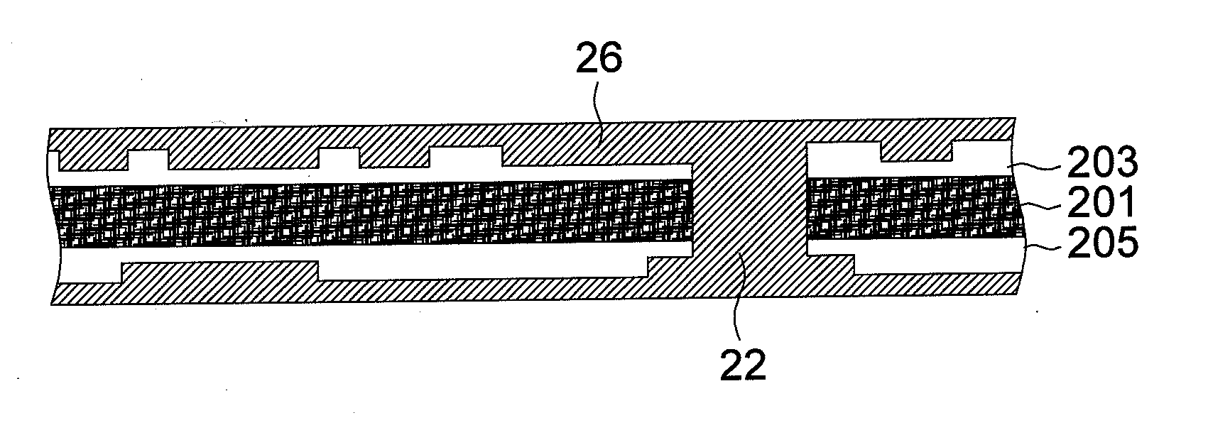
[0010]The invention is directed to an embedded-trace substrate structure and a method of manufacturing the same. A thick resin core plate is used for manufacturing a substrate structure with a uniform and smooth surface and a reduced overall thickness. The thinner appearance of the substrate of the invention indeed meets the requirements of products such as light weight, slimness and compactness in the commercial market.

Problems solved by technology

Thus, it is very difficult to achieve a high efficiency wiring on a BGA substrate.
Besides, in addition to the request of the flip chip technology, the request of systematic integration of the downstream products is also getting more and more urgent.
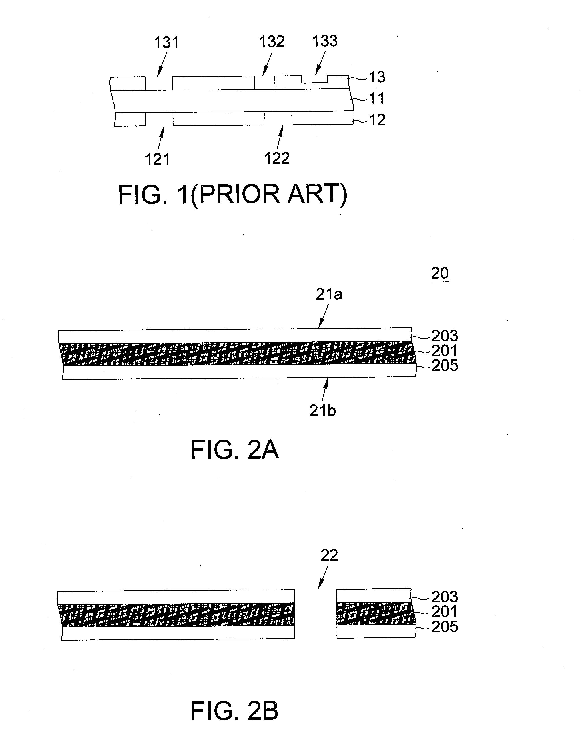
However, in the conventional type of integrated embedded-trace substrate of FIG. 1, the conductive pattern is projected from the central core 11 so the entire upper and the lower surfaces of the core plate are uneven.
Thus, the conventional integrated substrate structure as demonstrated in FIG. 1 is not suitable to be adopted in a small-sized product.
As the requirements of miniature and slimness are getting higher and higher, the product using the conventional substrate structure cannot satisfy the market requirements.

Method used


Image

  • Structure of embedded-trace substrate and method of manufacturing the same
  • Structure of embedded-trace substrate and method of manufacturing the same
  • Structure of embedded-trace substrate and method of manufacturing the same

Examples


Embodiment Construction

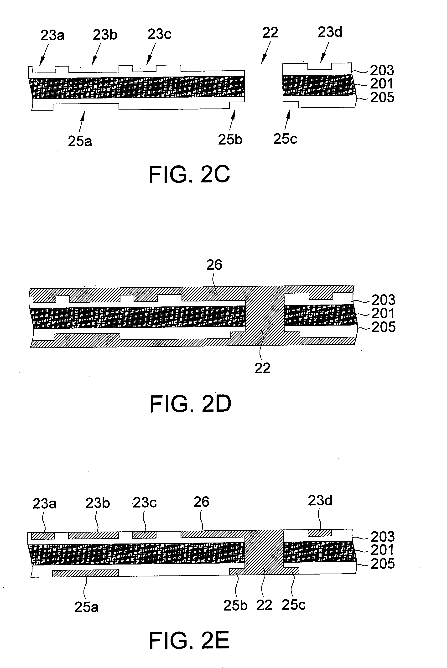
[0017]The invention provides a structure of embedded-trace substrate and a method of manufacturing the same. First, a surface of a thick resin core plate is patterned to form a through hole and a plurality of trenches for example. Next, one-plating step is applied for electroplating the through hole and the trenches with a conductive material at the same time. Then, the surface of the conductive material filling in the through hole and the trenches is processed to be coplanar with the surface of the core plate. Next, formation of solder mask layers and a surface treatment are conducted to complete an embedded-trace substrate of the invention. The embedded-trace substrate of the invention has reduced overall thickness, and the surface of the core plate is uniform and smooth (i.e. no conductive traces rising from the surface), which is very suitable to be used in small-sized products.

[0018]An embodiment is disclosed below for elaborating the manufacturing method of the embedded-trace ...


PUM

PropertyMeasurementUnit
trench widthaaaaaaaaaa
thicknessaaaaaaaaaa
thicknessaaaaaaaaaa

Abstract

A method of manufacturing an embedded-trace substrate is provided. First, a core plate is provided. Next, a through hole and a plurality of trenches are formed on the core plate, wherein the through hole passes through the core plate, and the trenches are formed on the upper and the lower surfaces of the core plate. Then, the core plate is subjected to one-plating step for electroplating a conductive material in the through hole and the trenches at the same time. Afterwards, the excess conductive material is removed.

Description

[0001]This application is a divisional application of co-pending U.S. application Ser. No. 12 / 647, 831, filed Dec. 28, 2009, which claims the benefit of Taiwan application Serial No. 98108656, filed Mar. 17, 2009. These related applications are incorporated herein by reference.BACKGROUND OF THE INVENTION[0002]1. Field of the Invention[0003]The invention relates in general to a structure of embedded-trace substrate and method of manufacturing the same, and more particularly to the double-layered embedded-trace substrate structure with thick resin core plate and a method of manufacturing the same.[0004]2. Description of the Related Art[0005]The integrated circuit (IC) package technology plays an important role in the electronics industry. An electronic packaging is for protecting and supporting circuit configuration, creating a path for heat dissipation and providing modularized standard specification for the parts. The electronic packaging 1990s mainly employs ball grid array (BGA) p...

Claims


Application Information

Patent Timeline
Patent Type & Authority Applications(United States)
IPC IPC(8): H05K3/00
CPCB32B17/04B32B27/04H05K1/036H05K3/045Y10T428/269H05K2201/0195H05K2201/029H05K3/0094H05K3/426B32B5/02B32B5/22B32B5/26B32B27/08B32B27/12B32B27/18B32B27/281B32B27/38B32B3/08B32B3/266B32B3/30B32B2255/00B32B2255/205B32B2260/021B32B2260/046B32B2262/101B32B2307/20B32B2307/202B32B2307/30B32B2307/718B32B2457/00
Inventor TARNG, SHIN-LUHLEE, TECK-CHONG
Owner ADVANCED SEMICON ENG INC
Learn More