Radiation sensor
- Summary
- Abstract
- Description
- Claims
- Application Information
AI Technical Summary
Benefits of technology
Problems solved by technology
Method used
Image

Examples
Embodiment Construction
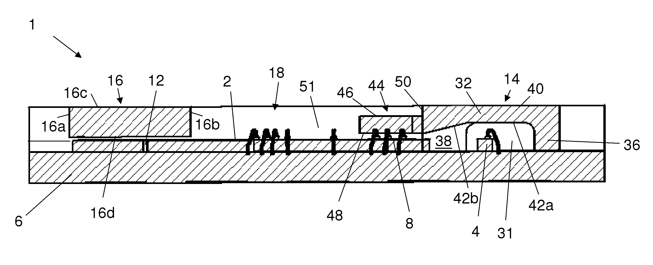
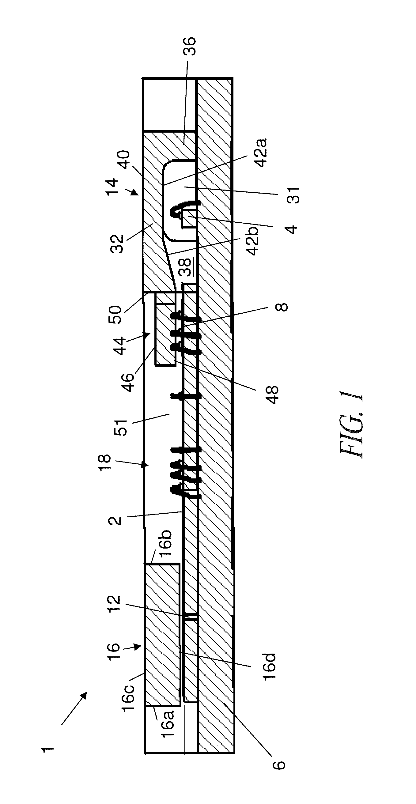
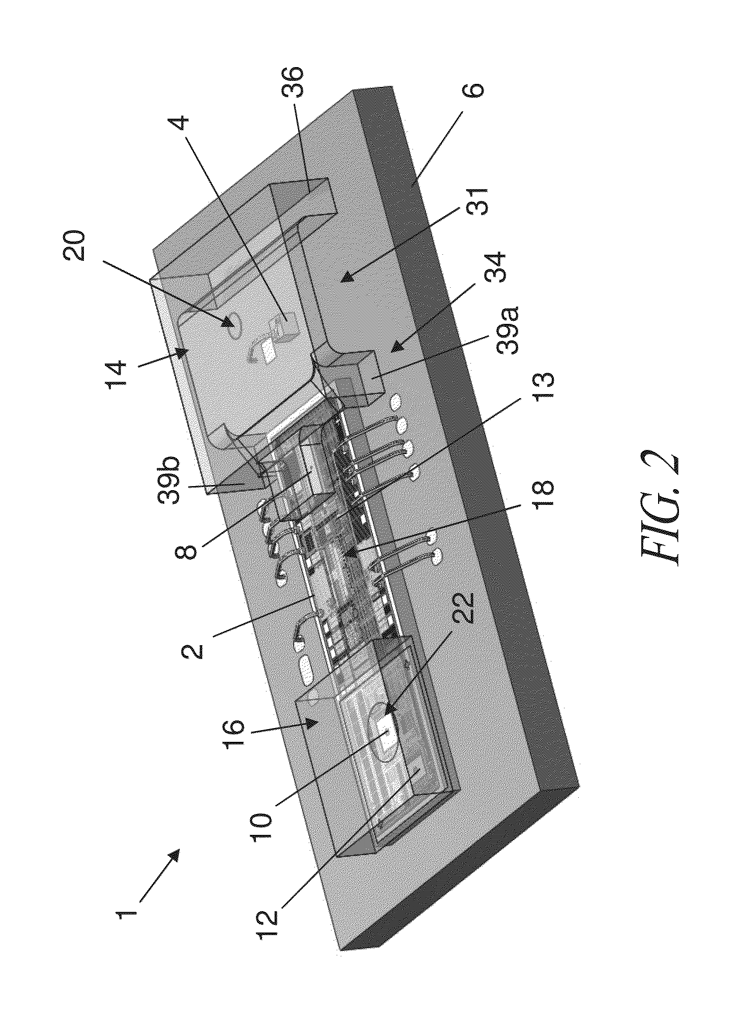
[0078]FIGS. 1-3 show a combined ambient radiation and proximity sensor 1 comprising a circuit board 2 and a radiation source 4 (such as an infrared LED or low power laser diode) mounted on a substrate 6. On the circuit board 2 is mounted a reference radiation detector 8, an ambient radiation detector 10, a returned radiation detector 12 and sensor control circuitry 13. The reference, ambient and returned radiation detectors 8, 10, 12 each typically comprise arrays of Single Photon Avalanche Detector (SPAD) pixels, but may alternatively comprise any suitable form of radiation detector (such as an array of complementary metal oxide semiconductor (CMOS) or charge coupled device (CCD) pixels).
[0079]A SPAD is based on a (typically CMOS) p-n junction device reverse biased beyond its breakdown region. The high reverse bias voltage generates a sufficient magnitude of electric field such that a single charge carrier introduced into the depletion layer of the device can cause a self-sustainin...
PUM
| Property | Measurement | Unit |
|---|---|---|
| Transparency | aaaaa | aaaaa |
| Time | aaaaa | aaaaa |
| Reflection | aaaaa | aaaaa |
Abstract
Description
Claims
Application Information
 - R&D
- Intellectual Property
- Life Sciences
- Materials
- Tech Scout
- Unparalleled Data Quality
- Higher Quality Content
- 60% Fewer Hallucinations
Browse by: Latest US Patents, China's latest patents, Technical Efficacy Thesaurus, Application Domain, Technology Topic, Popular Technical Reports.
© 2025 PatSnap. All rights reserved.Legal|Privacy policy|Modern Slavery Act Transparency Statement|Sitemap|About US| Contact US: help@patsnap.com