Eureka AIR delivers breakthrough ideas for toughest innovation challenges, trusted by R&D personnel around the world.

Low Noise CMOS Pixel Array

Inactive Publication Date: 2013-03-21
BAE SYST IMAGING SOLUTIONS
View PDF2 Cites 8 Cited by
  • Summary
  • Abstract
  • Description
  • Claims
  • Application Information

AI Technical Summary

Benefits of technology

The present invention is about an imaging array with multiple pixels. Each pixel has a photodetector, a floating diffusion node, a first amplification stage, and a select gate. A current minor is formed by the first and second amplification stages. The overall voltage gain of the current minor is between 0.9 and 1.1. The second amplification stage is shared by multiple pixels. This design provides a more efficient way of amplifying the light detected by the imaging array.

Problems solved by technology

However, the minimum size of the pixel depends on the charge-to-voltage conversion in the pixel and the noise levels in the pixel.
The source follower also contributes to the noise introduced in the image.
As the pixel size is reduced, the noise introduced by the source follower becomes significant.

Method used


Image

  • Low Noise CMOS Pixel Array
  • Low Noise CMOS Pixel Array
  • Low Noise CMOS Pixel Array

Examples


Embodiment Construction

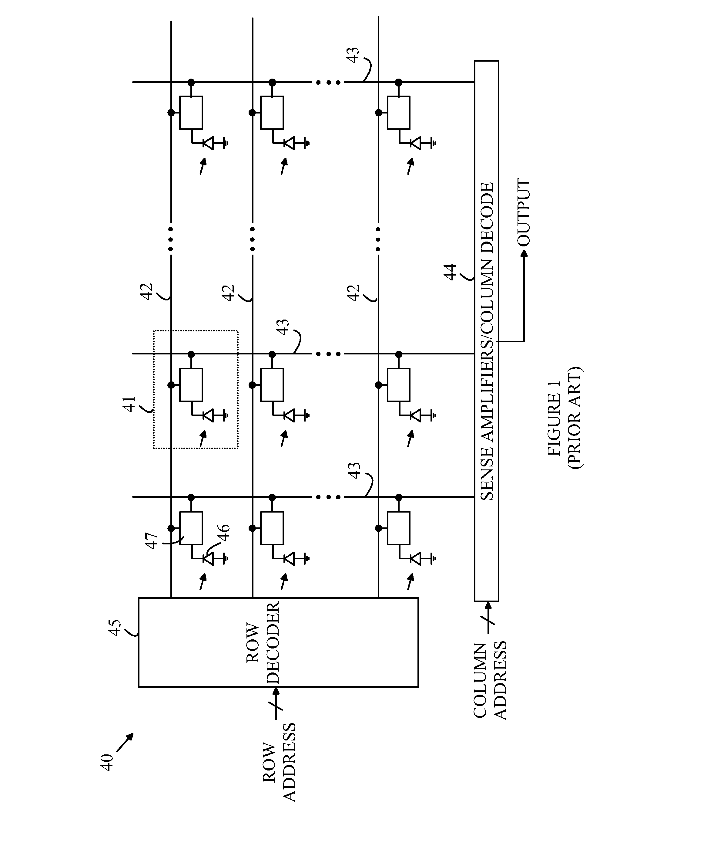
[0009]The manner in which the present invention provides its advantages can be more easily understood with reference to FIG. 1, which is a block diagram of a prior art CMOS imaging array. Imaging array 40 is constructed from a rectangular array of pixel cells 41. Each pixel cell includes a photodiode 46 and an interface circuit 47. The details of the interface circuit depend on the particular pixel design. However, all of the pixel circuits include a gate that is connected to a row line 42 that is used to connect that pixel to a bit line 43. The specific row that is enabled at any time is determined by a bit address that is input to a row decoder 45.

[0010]The various bit lines terminate in a column processing circuit 44 that typically includes sense amplifiers and column decoders. Each sense amplifier reads the signal produced by the pixel that is currently connected to the bit line processed by that sense amplifier. The sense amplifiers may generate a digital output signal by utili...


PUM


Abstract

An imaging array having a plurality of pixels is disclosed. Each pixel includes a photodetector that converts light to charge, a floating diffusion node, a first amplification stage connected to the floating diffusion node, and a select gate that connects the pixel to a second amplification stage. The first and second amplification stages form a current mirror. The first amplification stage includes a buried channel device. In one aspect of the present invention, the current minor has an overall voltage gain of between 0.9 and 1.1. In another aspect of the invention, the second amplification stage is shared by a plurality of pixels.

Description

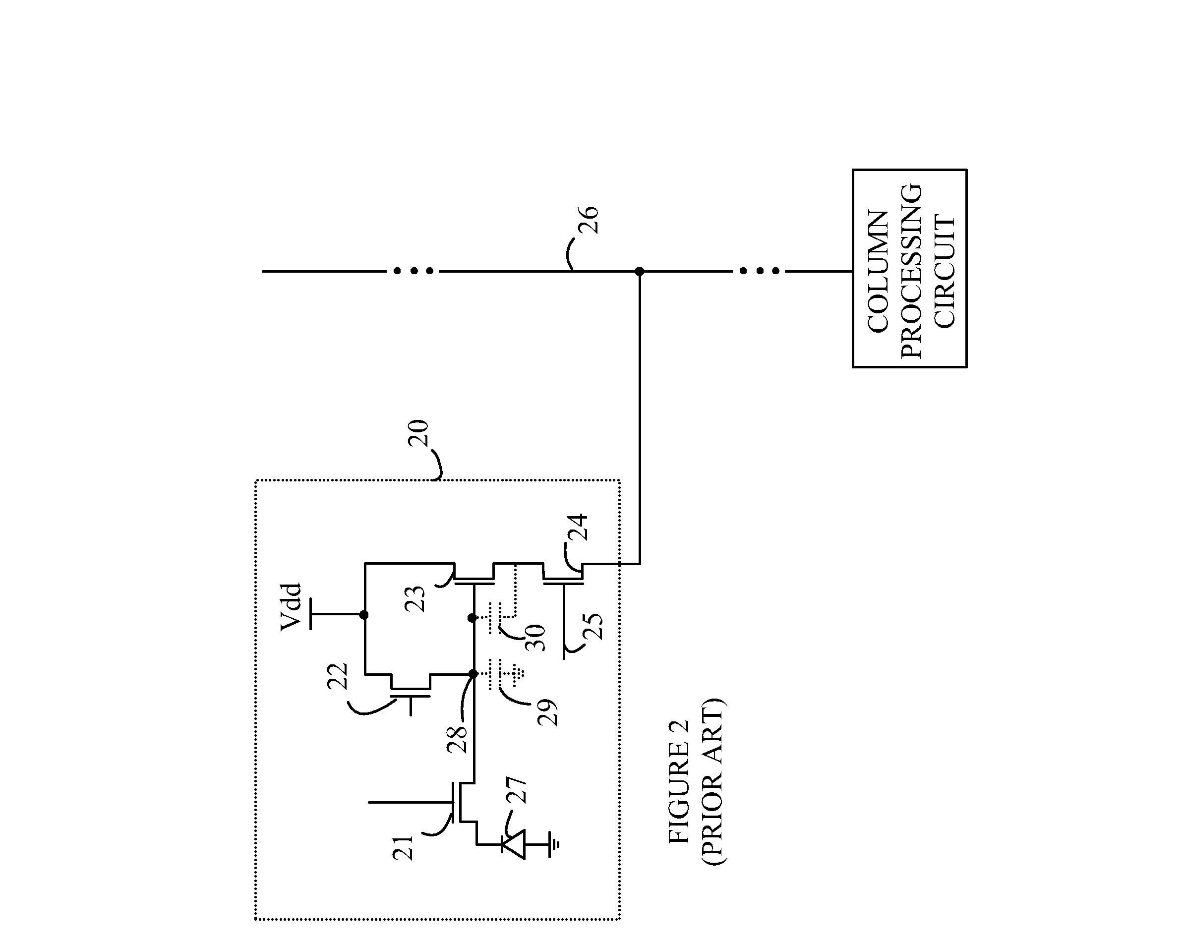
BACKGROUND OF THE INVENTION[0001]CMOS image sensors based on an active pixel design have gained wide acceptance in camera applications. In such sensors each pixel includes a photoreceptor that accumulates charge during an exposure. The accumulated charge is converted to a voltage by an output amplifier that is typically constructed from a source follower transistor that receives the charge at its gate and drives a bit line that is connected to the readout circuitry in the imaging array. The cost of the sensor is a direct function of the area of silicon needed for each pixel. To reduce the cost, pixel sizes have been reduced. However, the minimum size of the pixel depends on the charge-to-voltage conversion in the pixel and the noise levels in the pixel. Hence, pixels with high charge-to-voltage conversion factors and low noise are desired.[0002]The capacitance of the output stage determines the charge-to-voltage conversion ratio. Hence, arrangements that reduce this capacitance with...

Claims


Application Information

Patent Timeline
IPC IPC(8): H04N5/335
CPCH04N5/3745H04N5/363H04N25/65H04N25/77
Inventor FOWLER, BOYDLIU, XINGZAO
Owner BAE SYST IMAGING SOLUTIONS
Why Eureka
Eureka Blog
Learn More