
Laminated and sintered ceramic circuit board, and semiconductor package including the circuit board

a technology of laminated and sintered ceramics and circuit boards, which is applied in the manufacture of printed circuits, printed circuit aspects, metallic pattern materials, etc., can solve the problems of wiring (disconnection, reliability decline), etc., and achieve low open failure rate, high reliability, and fast

Active Publication Date: 2013-02-28
NGK INSULATORS LTD
View PDF0 Cites 9 Cited by
  • Summary
  • Abstract
  • Description
  • Claims
  • Application Information

AI Technical Summary

Benefits of technology

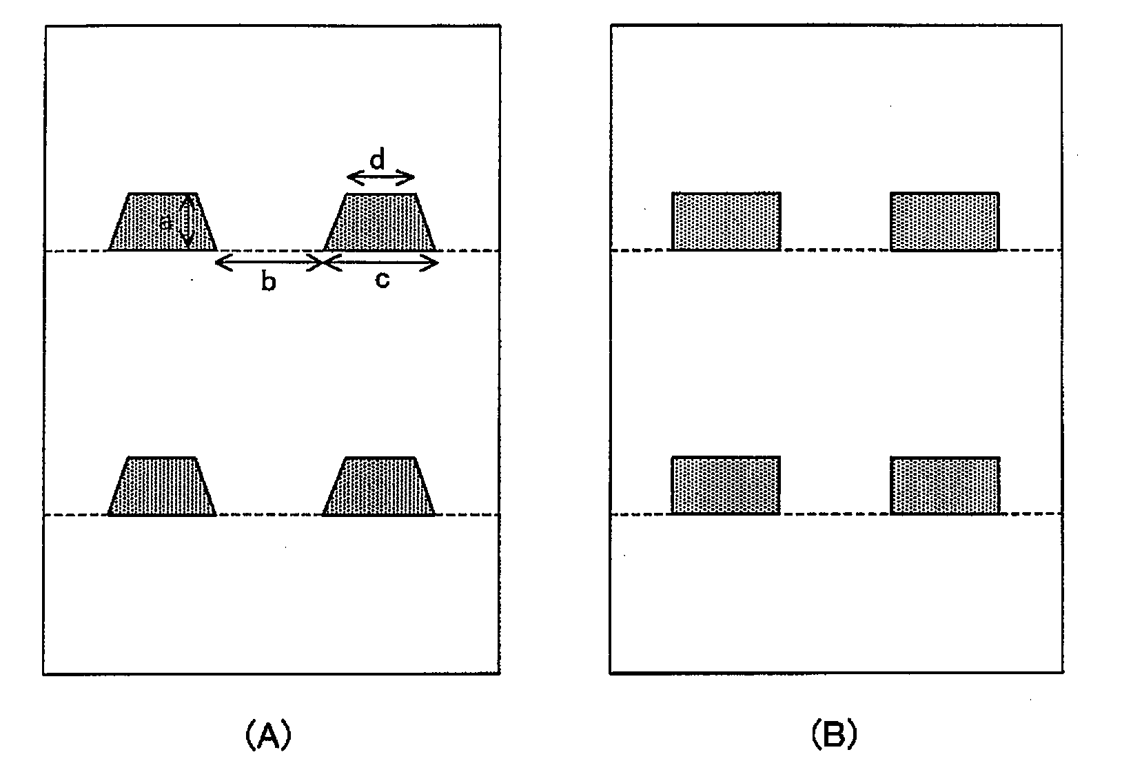
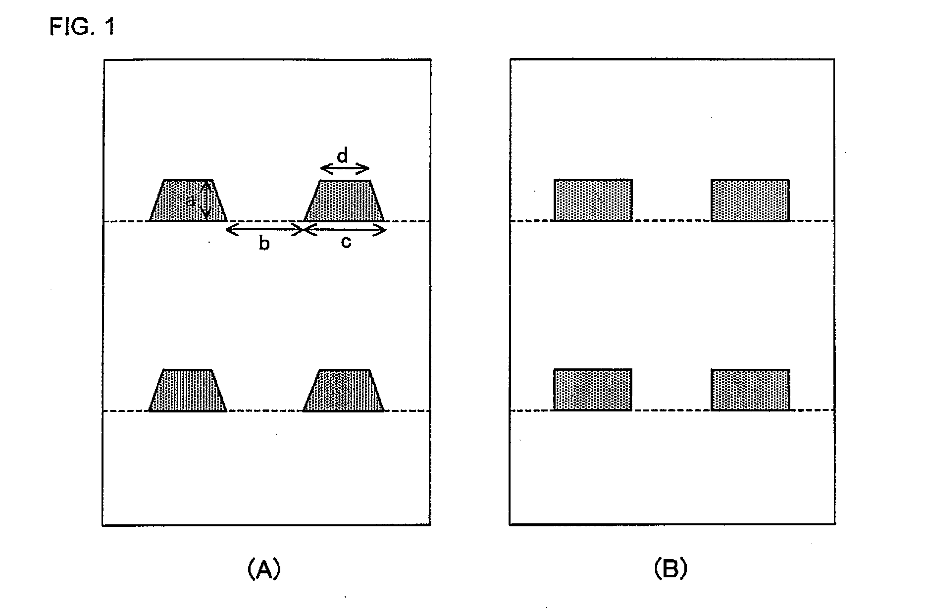
The present invention provides a laminated ceramic circuit board with fine-lined wiring layers that have a low open failure rate and high reliability against high temperature and high humidity. The circuit board has a trapezoidal shape with certain dimensions and a specific relation between the cross-section of adjacent inplane conductors. A semiconductor package using this circuit board is fast, downsized, and thin with high reliability.

Problems solved by technology

Therefore, the inventors manufactured circuit boards with line widths and line intervals in a wiring layer of 15 μm or less by way of trial, evaluated and reviewed the same, and then problems such as frequent occurrences of open of wiring (disconnection) and decrease in reliability under high temperature and high humidity environment occurred.

Method used


Image

  • Laminated and sintered ceramic circuit board, and semiconductor package including the circuit board
  • Laminated and sintered ceramic circuit board, and semiconductor package including the circuit board
  • Laminated and sintered ceramic circuit board, and semiconductor package including the circuit board

Examples


first embodiment

is the present invention.

[0054]As described above, the laminated and sintered ceramic circuit board according to the present embodiment comprises a base material comprising a plurality of dielectric layers of ceramic. As mentioned previously, ceramic has a coefficient of thermal expansion close to that of silicon constituting a semiconductor element. Accordingly, in the laminated and sintered ceramic circuit board according to the present embodiment, even when the board in a condition where it is joined with a semiconductor element is exposed to temperature alteration as mentioned previously, the difference between dimension change of the semiconductor element and that of the board is small. As a result, in the laminated and sintered ceramic circuit board according to the present embodiment, thermal stress acting between the semiconductor element and the board can be suppressed.

[0055]Thereby, problems such as breakdown of a joining part between a semiconductor element and a board, d...

second embodiment

is the present invention.

[0090]As described above, the laminated and sintered ceramic circuit board according to the present embodiment is configured so that the ratio (d / c) of the length (d) of the upper base to the length (c) of the lower base of the trapezoidal cross-section surfaces of inplane conductors constituting the fine-lined inplane wiring is −1 / 2*(a / b)+0.93 or more, and −1 / 2*(a / b)+1.10 or less. Thereby, detachment and lack of conductor pattern as mentioned previously, and void at a corner portion formed by the side surfaces of conductor patterns and the surface of protective substrate or green sheet become more unlikely to occur. As a result, the laminated and sintered ceramic circuit board according to the present embodiment can further decrease problems such as open failure, decrease in reliability against high temperature and high humidity and the like.

[0091]By the way, a method for manufacturing the laminated and sintered ceramic circuit boards according to the previ...

seventh embodiment

is the present invention.

[0139]In addition, as a more preferable embodiment, the semiconductor package according to the seventh embodiment of the present invention, wherein:

[0140]the height (a), the interval (b), the length (c) of the lower base and the length (d) of the upper base of the trapezoidal cross-section of inplane conductors constituting the fine-lined inplane wiring meet the relation represented by the following formula (3):

-12×ab+0.93≤dc,dc≤-12×ab+1.10(3)


PUM


Abstract

In the laminated and sintered ceramic circuit board according to the present invention, at least a portion of the inplane conductor is fine-lined, such that the shape of the cross-section surface of the fine-lined inplane conductor is trapezoid, and the height (a), the length (c) of the lower base and the length (d) of the upper base of the trapezoidal cross-section surfaces, and the interval (b) between the lower bases of the trapezoidal cross-section surfaces of the inplane conductors adjacent in a plane parallel to the principal surfaces of the board meet a certain relation. This provides a laminated ceramic circuit hoard with low open failure rate, short-circuit failure rate and high reliability against high temperature and high humidity in a downsized and short-in-height (thin) semiconductor package.

Description

BACKGROUND OF THE INVENTION[0001]1. Field of the Invention[0002]The present invention relates to a laminated and sintered ceramic circuit board. Specifically, the present invention relates to a laminated and sintered ceramic circuit board having a fine-lined inner layer wiring. Further, the present invention also relates to a semiconductor package including the laminated and sintered ceramic circuit board.[0003]2. Description of the Related Art[0004]Conventionally, semiconductor packages such as so-called flip-chip BGA packages, in which a semiconductor element such as an IC chip and the like is joined on a circuit board by flip-chip mounting or the like and sealed with molding compound such as resin and the like, are commonly used. Resin circuit boards for such semiconductor packages generally consist of multilayer board, in which plural wiring layers and insulation layers are laminated and the wiring layers and through conductor extending through the insulation layers electrically...

Claims


Application Information

Patent Timeline
IPC IPC(8): H01L23/48H05K1/09H05K1/00
CPCH05K3/4623H05K3/4629H05K2201/09827H01L23/49827H01L2924/0002H01L23/5226H01L2924/00H01L23/49838H01L23/5283H05K2201/09227H05K2201/09236H05K2201/098H05K1/0242H01L23/49822
Inventor TANI, MAKOTOHIRAI, TAKAMIYANO, SHINSUKETANABE, DAISHI
Owner NGK INSULATORS LTD
Learn More