Differential sense amplifier without dedicated pass-gate transistors
a technology of pass-gate transistor and sense amplifier, which is applied in the field of sense amplifier, can solve the problems of increasing the area of the entire circuit and its fabrication cost, and achieve the effect of simple and robust memory sense amplifier
- Summary
- Abstract
- Description
- Claims
- Application Information
AI Technical Summary
Benefits of technology
Problems solved by technology
Method used
Image
Examples
first embodiment
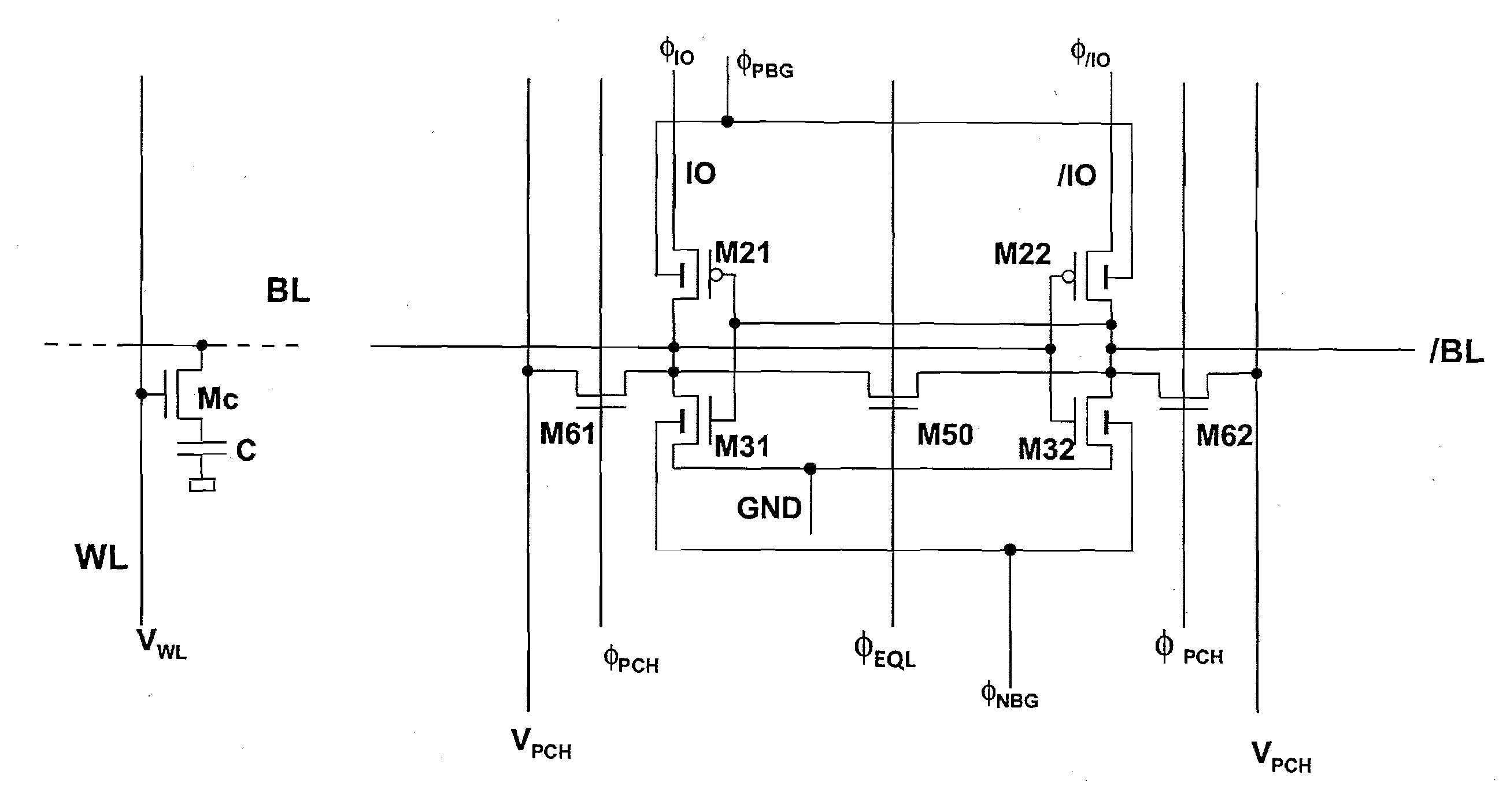
[0079]As illustrated in FIG. 3, a sense amplifier according to the first embodiment of the invention includes four transistors M21, M22, M31, M32 for the inverters, with two additional precharge transistors M61, M62 and one additional equalization transistor M50.
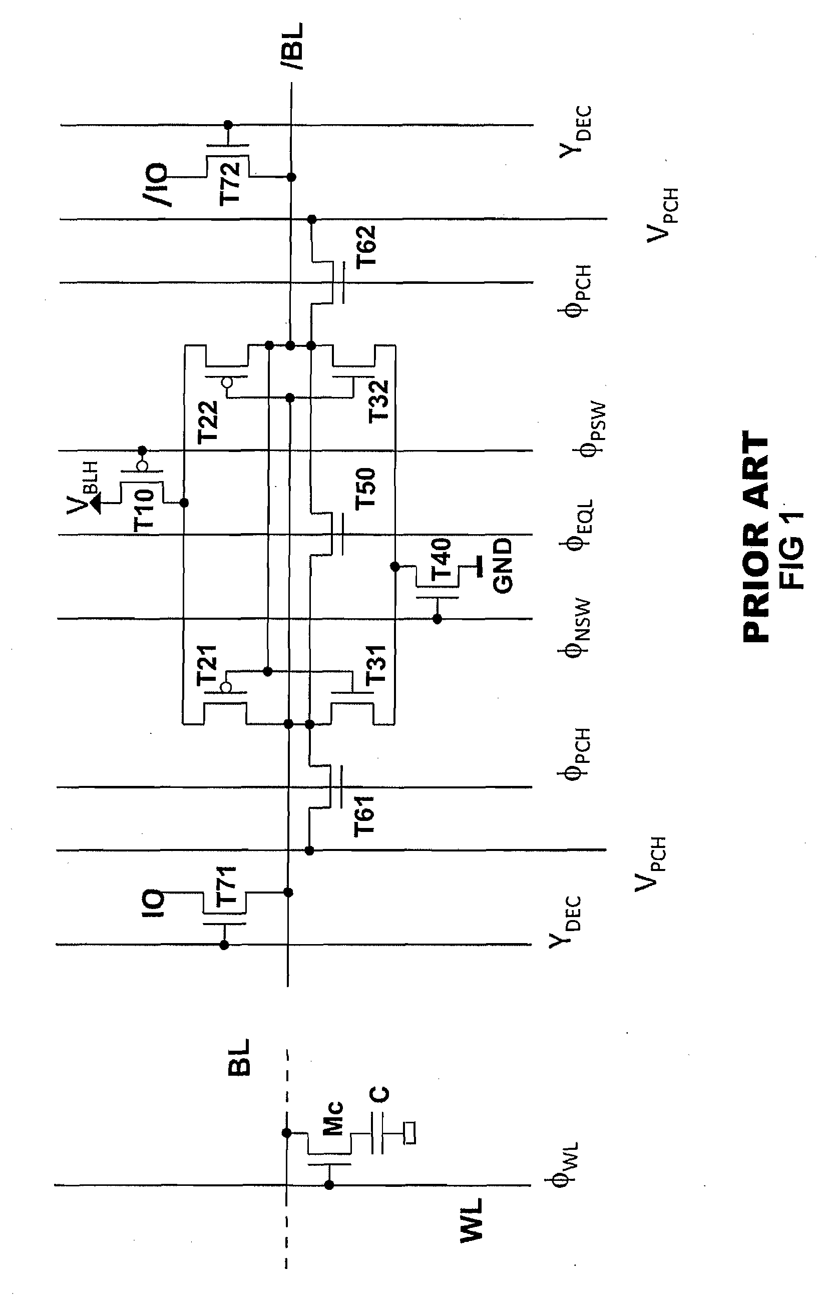
[0080]As for FIG. 1 illustrating a prior art sense amplifier, and for simplicity's sake, only one word line WL and one memory cell C are shown on the left hand side of the sense amplifier. The cell C is addressed by the word line WL that controls the gate of a cell access transistor Mc, the cell access transistor Mc connecting the memory cell C to a bit line.
[0081]The differential sense amplifier for sensing data stored in a plurality of memory cells C of a memory cell array according to the first embodiment comprises:[0082]a first CMOS inverter having an output connected to a first bit line BL and an input connected to a second bit line / BL complementary to the first bit line BL,[0083]a second CMOS inverter having an output...
second embodiment
No Switch Transistors, no Dedicated Precharge Transistors and no Dedicated Pass-gate Transistors
[0144]As illustrated in FIG. 5, a sense amplifier according to the second embodiment of the invention includes four transistors M21, M22, M31, M32 for the inverters and one additional equalization transistor M50.
[0145]The sense amplifier of FIG. 5 comprises:[0146]a first CMOS inverter having an output connected to a first bit line BL and an input connected to a second bit line / BL complementary to the first bit line BL,[0147]a second CMOS inverter having an output connected to the second bit line / BL and an input connected to the first bit line BL.
Each CMOS inverter comprises:[0148]a pull-up transistor M21, M22 having a drain and a source, and[0149]a pull-down transistor M31, M32 having a drain and a source, with the pull-up transistor M21, M22 and the pull-down transistor M31, M32 of each CMOS inverter having a common drain.
[0150]In the depicted embodiment of FIG. 5, the pull-up transist...
PUM
 Abstract
Description
Claims
Application Information
 - R&D
- Intellectual Property
- Life Sciences
- Materials
- Tech Scout
- Unparalleled Data Quality
- Higher Quality Content
- 60% Fewer Hallucinations
Browse by: Latest US Patents, China's latest patents, Technical Efficacy Thesaurus, Application Domain, Technology Topic, Popular Technical Reports.
© 2025 PatSnap. All rights reserved.Legal|Privacy policy|Modern Slavery Act Transparency Statement|Sitemap|About US| Contact US: help@patsnap.com


