Integrated circuit packaging system for electromagnetic interference shielding and method of manufacture thereof
- Summary
- Abstract
- Description
- Claims
- Application Information
AI Technical Summary
Problems solved by technology
Method used
Image
Examples
first embodiment
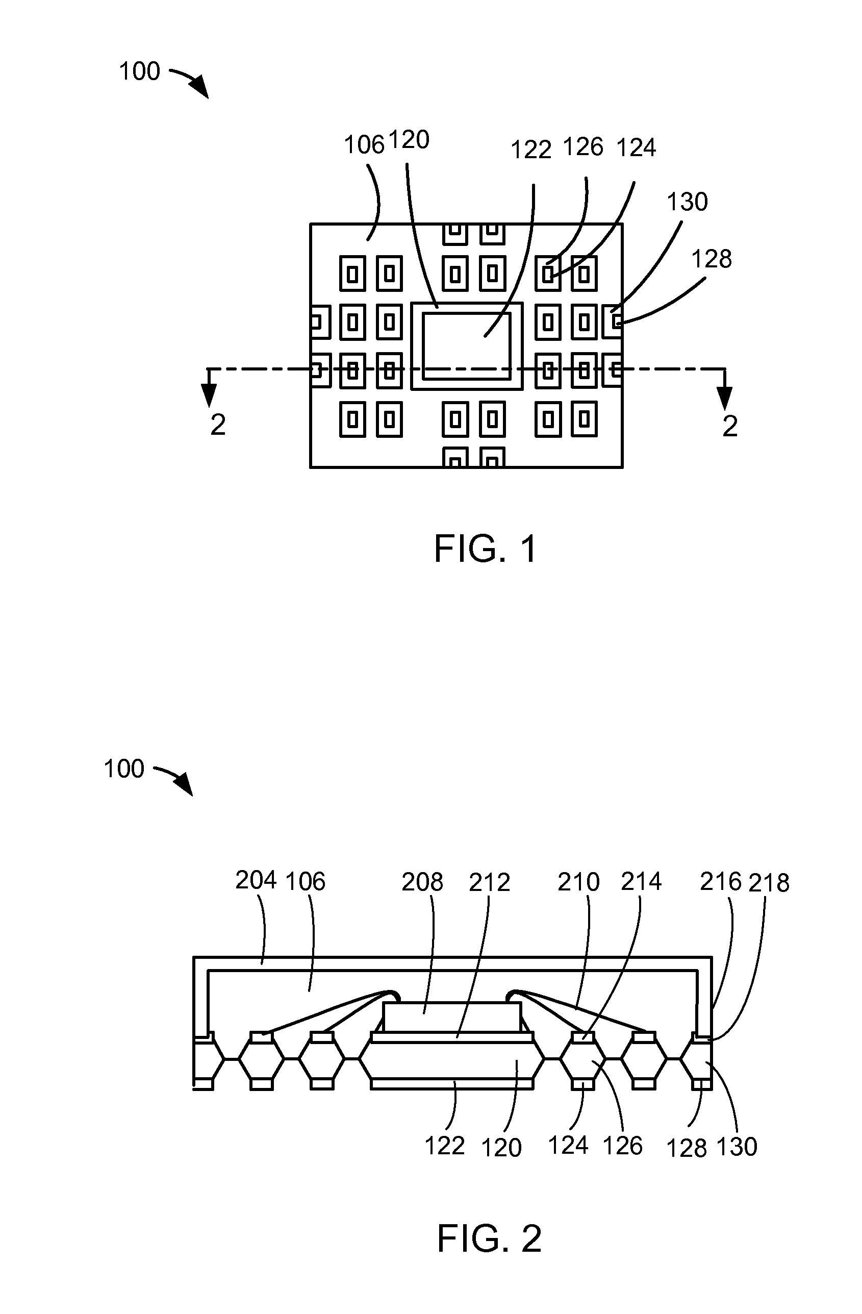
[0039]Referring now to FIG. 1, therein is shown a bottom view of an integrated circuit packaging system 100 in the present invention. The integrated circuit packaging system 100 can be an integrated circuit package having an electromagnetic interference (EMI) shielding.
[0040]The integrated circuit packaging system 100 can include an encapsulation 106. The encapsulation 106 is a cover providing electrical and environmental protections to the structure within the encapsulation 106, such as a protective covering. As an example, the encapsulation 106 can be formed by molding an encapsulation material such as epoxy molding compound or other insulating resin material.
[0041]The integrated circuit packaging system 100 can include a die attach paddle 120, a die attach paddle contact pad 122, an inner lead 126, an inner lead contact pad 124, a peripheral lead 130, and a peripheral lead contact pad 128. The die attach paddle 120 is a structural element for supporting an integrated circuit.
[004...
second embodiment
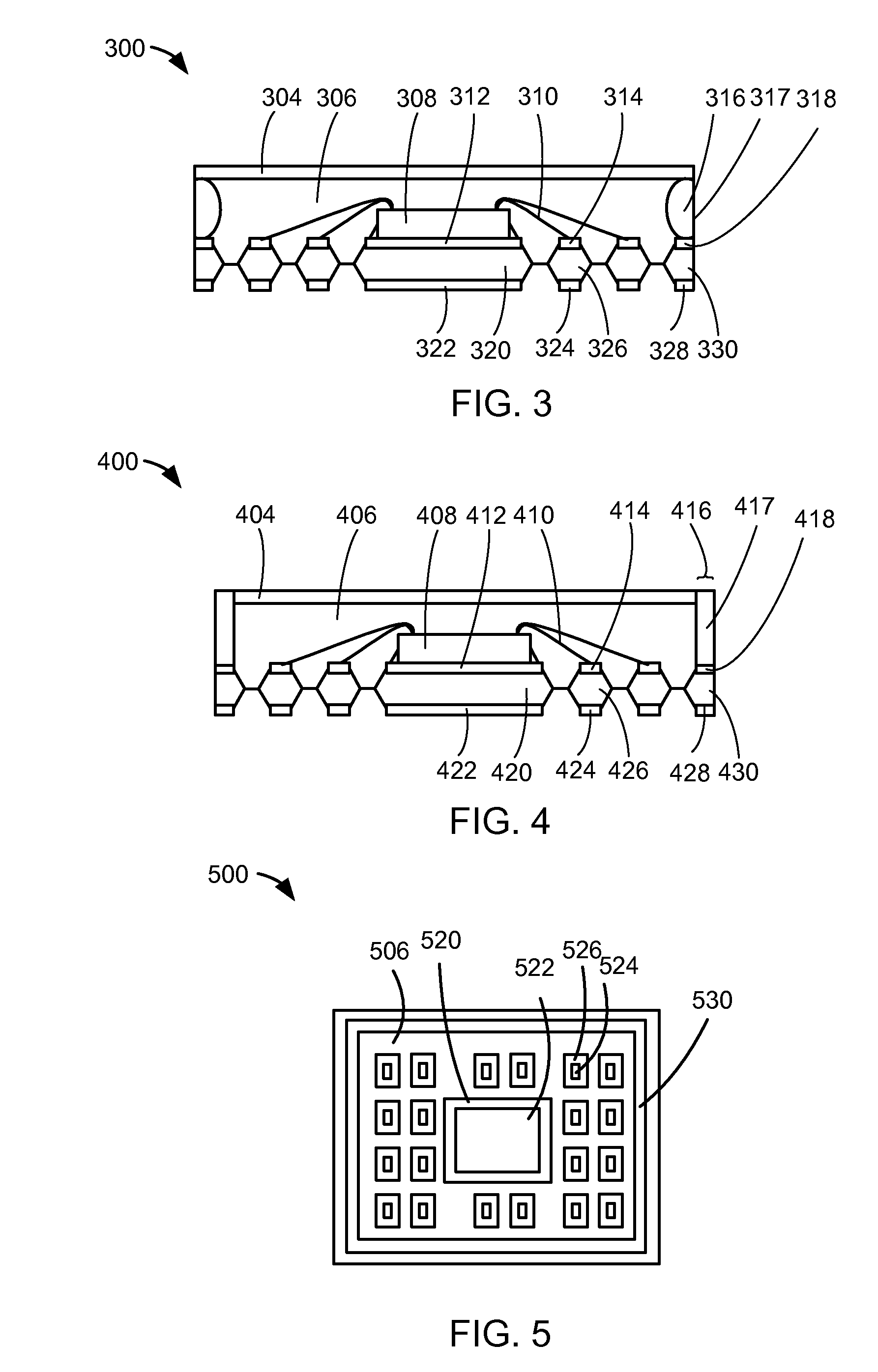
[0050]Referring now to FIG. 3, therein is shown a cross-sectional view of an integrated circuit packaging system as exemplified by the bottom view of FIG. 1 along a line 2-2 of FIG. 1 in the present invention. The second cross-sectional view of an integrated circuit packaging system 300 depicts a conductive shielding layer 304 coupled to a peripheral lead 330 with a peripheral interconnect 316.
[0051]The integrated circuit packaging system 300 can include a die attach paddle pad 312, an inner lead pad 314, and a peripheral lead pad 318. The die attach paddle pad 312, the inner lead pad 314, and the peripheral lead pad 318 are conductive elements that can be used to mount components or interconnections. The die attach paddle pad 312, the inner lead pad 314, and the peripheral lead pad 318 can be formed of an etch-resistant material, such as a nickel-chromium alloy.
[0052]An integrated circuit 308 can be mechanically coupled to a die attach paddle 320 by an adhesive, such as a die attac...
third embodiment
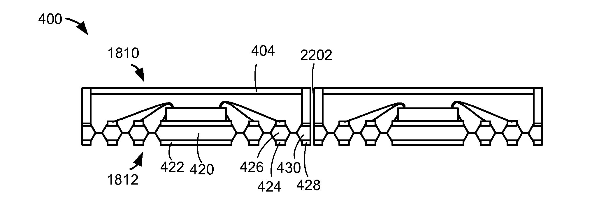
[0058]Referring now to FIG. 4, therein is shown a cross-sectional view of an integrated circuit packaging system as exemplified by the bottom view of FIG. 1 along a line 2-2 of FIG. 1 in the present invention. The second cross-sectional view of an integrated circuit packaging system 400 can include a conductive shielding layer 404 coupled to a peripheral lead 430 with a conductive paste plug 416.
[0059]The integrated circuit packaging system 400 can include a die attach paddle pad 412, an inner lead pad 414, and a peripheral lead pad 418. The die attach paddle pad 412, the inner lead pad 414, and the peripheral lead pad 418 are conductive elements that can be used to mount components or interconnections. The die attach paddle pad 412, the inner lead pad 414, and the peripheral lead pad 418 can be formed of an etch-resistant material, such as a nickel-chromium alloy.
[0060]An integrated circuit 408 can be mechanically coupled to a die attach paddle 420 by an adhesive, such as a die att...
PUM
 Abstract
Description
Claims
Application Information
 - R&D
- Intellectual Property
- Life Sciences
- Materials
- Tech Scout
- Unparalleled Data Quality
- Higher Quality Content
- 60% Fewer Hallucinations
Browse by: Latest US Patents, China's latest patents, Technical Efficacy Thesaurus, Application Domain, Technology Topic, Popular Technical Reports.
© 2025 PatSnap. All rights reserved.Legal|Privacy policy|Modern Slavery Act Transparency Statement|Sitemap|About US| Contact US: help@patsnap.com


