
Wafer susceptor and chemical vapor deposition apparatus

Inactive Publication Date: 2012-09-27
CHI MEI LIGHTING TECH
View PDF0 Cites 15 Cited by
  • Summary
  • Abstract
  • Description
  • Claims
  • Application Information

AI Technical Summary

Benefits of technology

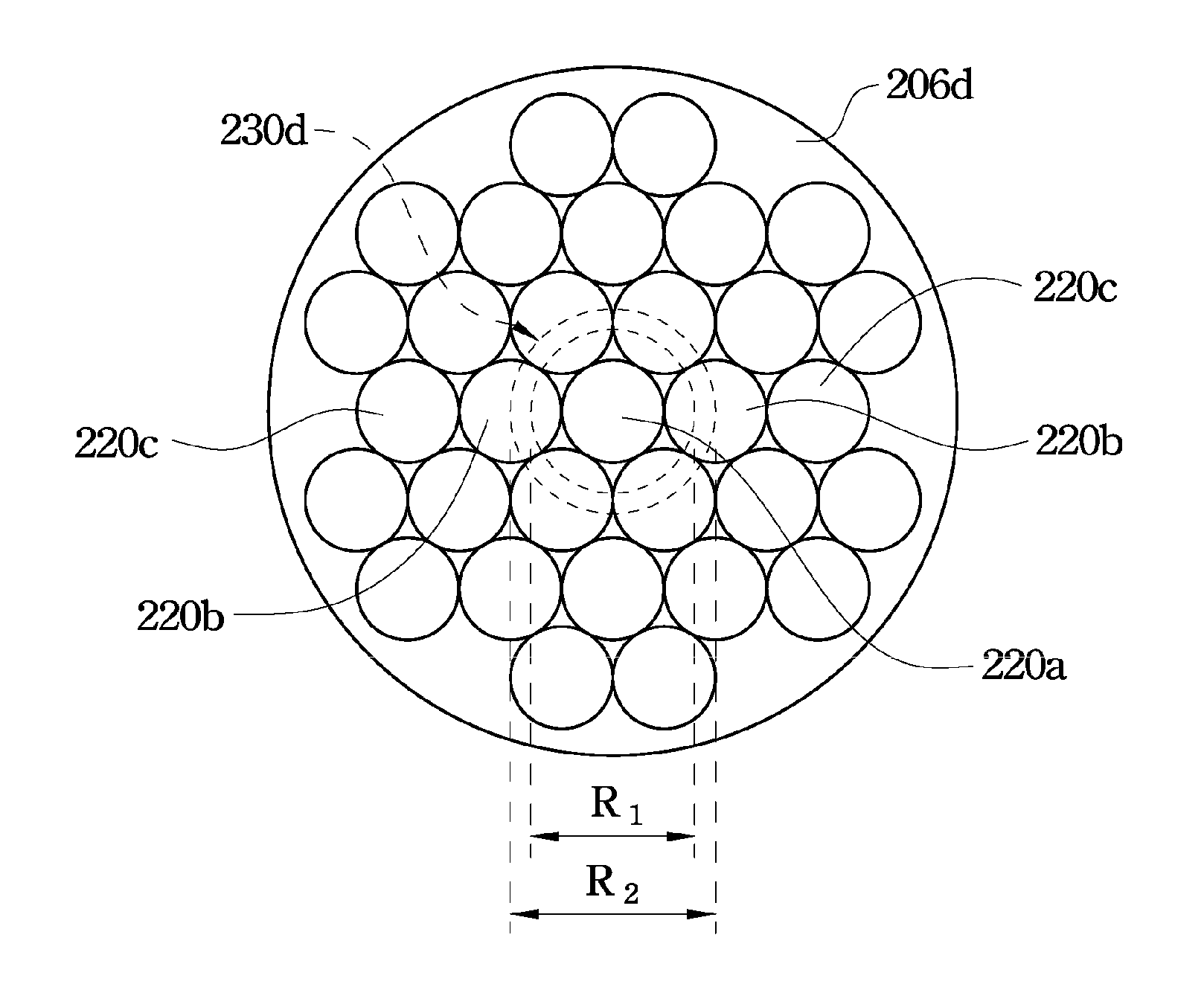
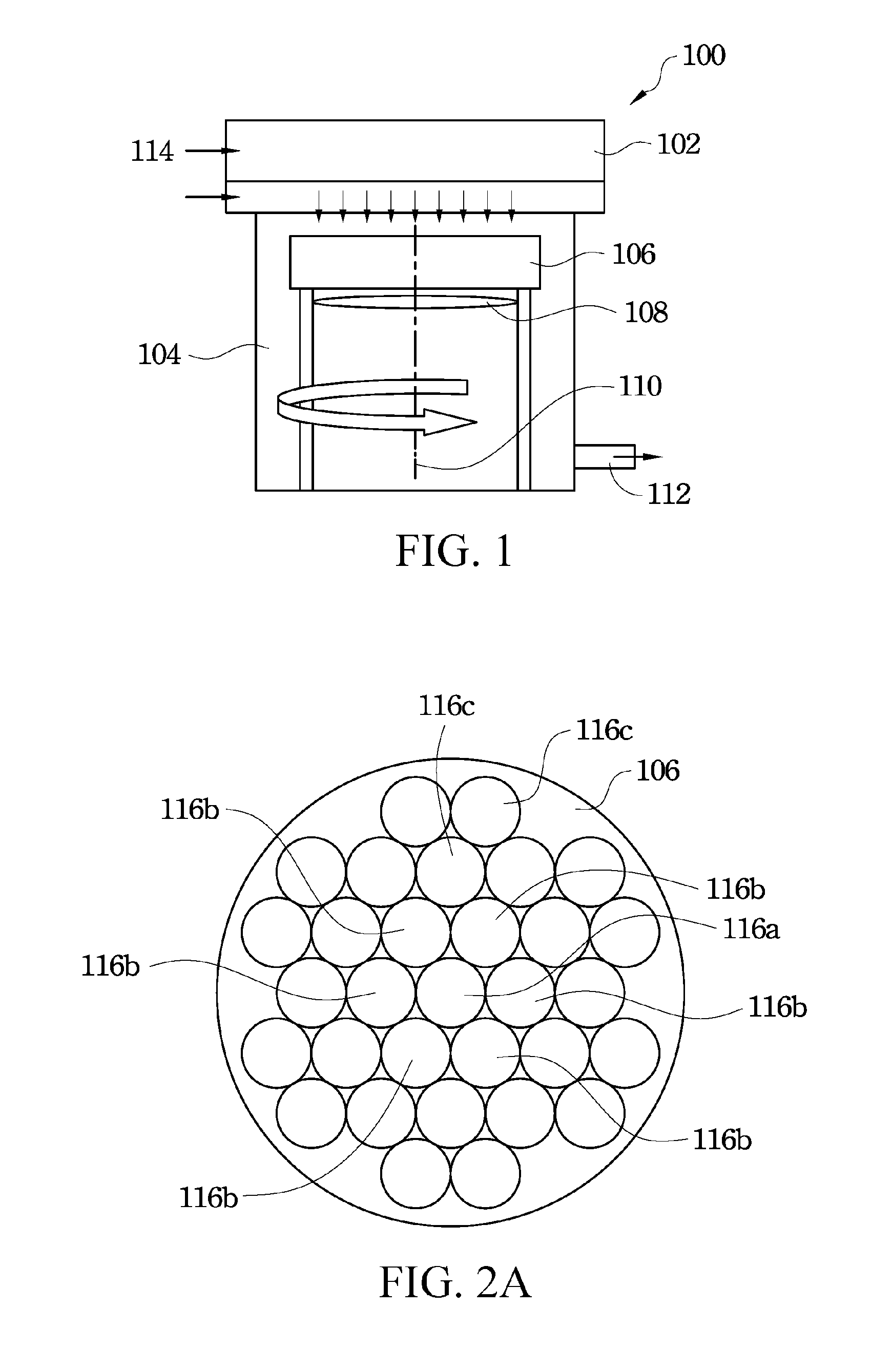
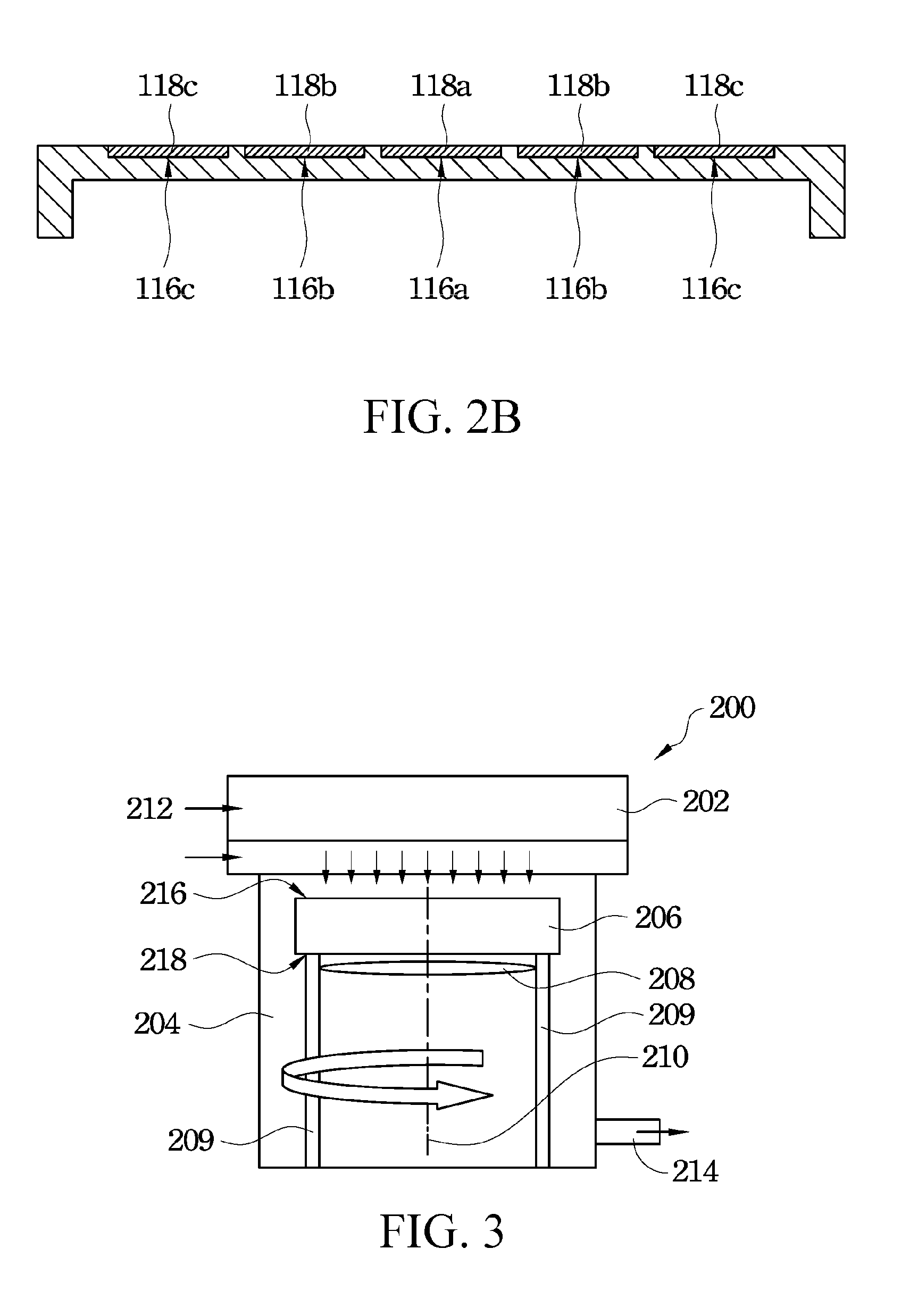
[0010]Accordingly, in one aspect, the present invention is directed to a wafer susceptor and a CVD apparatus, in which a recessed portion is disposed at a central area of the susceptor, so that the susceptor has different thickness distribution. Thus, the problem of uneven temperature of the susceptor can be effectively solved.
[0011]In another aspect, the present invention is directed to a wafer susceptor and a CVD apparatus, which can effectively solve the problem that the characteristics and the wavelength of chips placed at a central area of the susceptor are abnormal.
[0012]In a further aspect, the present invention is also directed to a wafer susceptor and a CVD apparatus, which can improve the uniformity of temperature distribution of the susceptor, thereby improving the consistency of the characteristics of chips of the same production batch, and achieving the purpose of improving the production yield.
[0023]By application of the wafer susceptor and the CVD apparatus of the present invention, among other things, the problem of uneven temperature of a susceptor can be effectively solved, and the problem that the characteristics and wavelength of chips placed at a central area of the susceptor are abnormal can be solved, so as to improve the consistency of the characteristics of chips of the same production batch.

Problems solved by technology

Thus, the characteristics of the chips of the same production batch are not consistent, thereby resulting in the yield loss.
Therefore, a heretofore unaddressed need exists in the art to address the aforementioned deficiencies and inadequacies.

Method used


Image

  • Wafer susceptor and chemical vapor deposition apparatus
  • Wafer susceptor and chemical vapor deposition apparatus
  • Wafer susceptor and chemical vapor deposition apparatus

Examples


Embodiment Construction

[0037]The present invention will now be described more fully hereinafter with reference to the accompanying drawings, in which exemplary embodiments of the invention are shown. This invention may, however, be embodied in many different forms and should not be construed as limited to the embodiments set forth herein. Rather, these embodiments are provided so that this disclosure will be thorough and complete, and will fully convey the scope of the invention to those skilled in the art. Like reference numerals refer to like elements throughout.

[0038]The terminology used herein is for the purpose of describing particular embodiments only and is not intended to be limiting of the invention. As used herein, the singular forms “a”, “an” and “the” are intended to include the plural forms as well, unless the context clearly indicates otherwise. It will be further understood that the terms “comprises” and / or “comprising,” or “includes” and / or “including” or “has” and / or “having” when used he...


PUM

PropertyMeasurementUnit
Timeaaaaaaaaaa
Thicknessaaaaaaaaaa
Thicknessaaaaaaaaaa

Abstract

A wafer susceptor and a chemical vapor deposition apparatus. In one embodiment, the chemical vapor deposition apparatus includes a chamber, a susceptor, a heater and a gas supply system. The susceptor is disposed within the chamber and is rotatable around a rotation axis, wherein an upper surface of the susceptor is suitable for carrying a plurality of wafers, and a middle region of a lower surface of the susceptor is set with a first cavity. The heater is disposed under the susceptor and is used to heat the wafers on the susceptor. The gas supply system is used to introduce a reactive gas into the chamber.

Description

CROSS-REFERENCE TO RELATED APPLICATIONS[0001]This non-provisional application claims priority under 35 U.S.C. §119(a) on Patent Application No. 100109747 filed in Taiwan, R.O.C. on Mar. 22, 2011, the entire contents of which are hereby incorporated by reference.FIELD OF THE INVENTION[0002]The present invention relates to a deposition apparatus, and more particularly to a chemical vapor deposition (CVD) apparatus.BACKGROUND OF THE INVENTION[0003]Presently, in processes for manufacturing compound semiconductor devices, a Chemical Vapor Deposition (CVD) apparatus, such as a metal-organic CVD (MOCVD), is usually used for growing chips required. The existing CVD apparatuses are classified into vertical type and horizontal type according to different design forms of a reaction chamber. The vertical type CVD apparatus is such designed that a precursor required for deposition reaction is introduced to a position above chips in the reaction chamber in a manner of being vertical to the chip s...

Claims


Application Information

Patent Timeline
IPC IPC(8): C23C16/458B05C13/00
CPCC23C16/4584H01L21/68771H01L21/68764
Inventor CHEN, WEICHENGLEE, ZONGLINWANG, HSINCHUAN
Owner CHI MEI LIGHTING TECH
Learn More