
Light-emitting diode package

Inactive Publication Date: 2012-08-16
GENESIS PHOTONICS
View PDF1 Cites 0 Cited by
  • Summary
  • Abstract
  • Description
  • Claims
  • Application Information

AI Technical Summary

Benefits of technology

[0008]Therefore, the object of the present invention is to provide a light-emitting diode package that can simplify the manufacturing process thereof and that can overcome the drawback of inferior heat dissipation.

Problems solved by technology

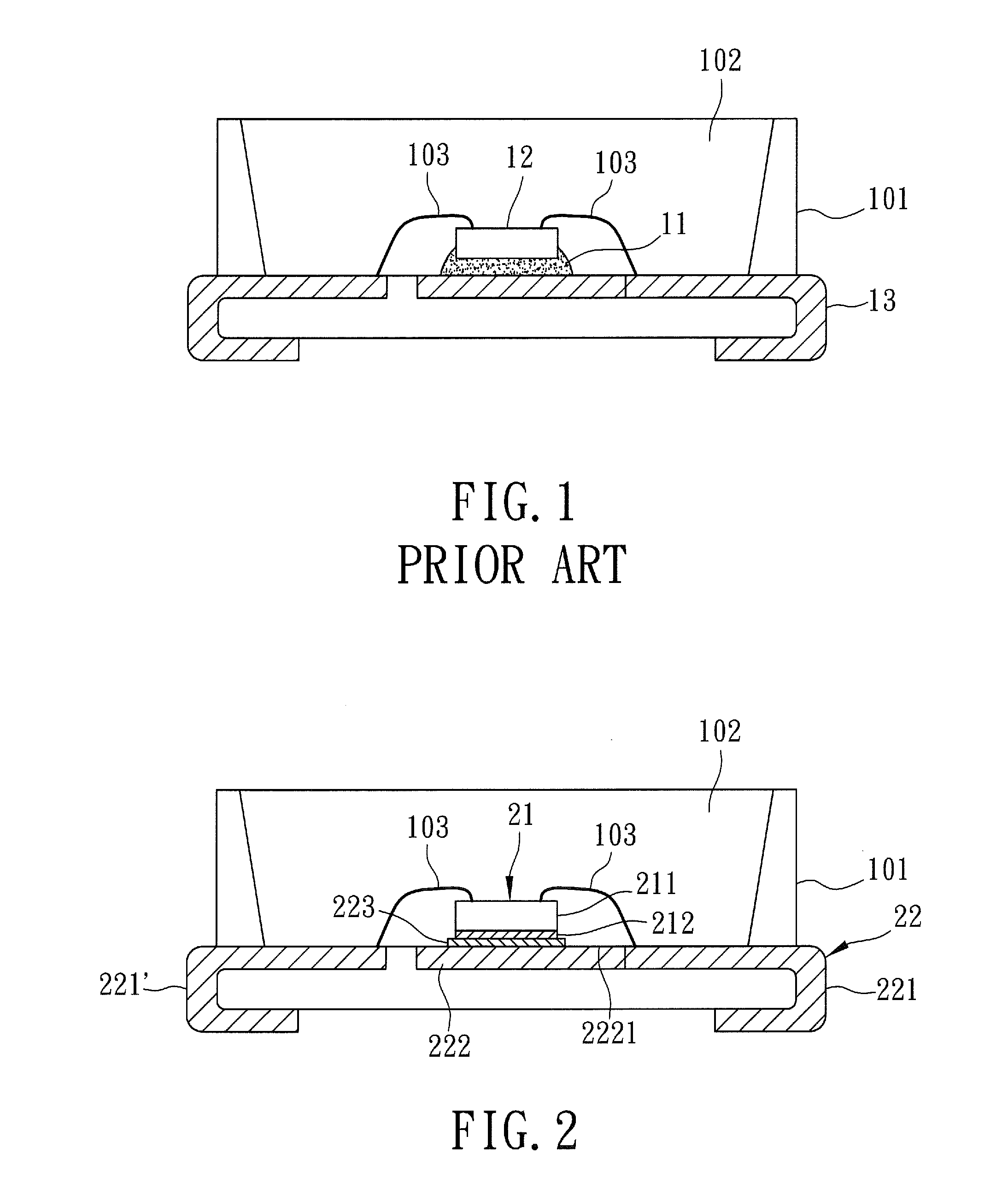
Since the precise positioning of the light-emitting diode chip 12 and the baking process are required, the manufacturing process of the conventional light-emitting diode package is relatively complicated.
However, because the thermal conductivity coefficient of the adhesive 11 is generally low, the heat-dissipating effect is poor, thereby adversely affecting the service lifetime of the light-emitting diode package.

Method used


Image

  • Light-emitting diode package
  • Light-emitting diode package
  • Light-emitting diode package

Examples


Embodiment Construction

[0016]Before the present invention is described in greater detail, it should be noted that like components are assigned the same reference numerals throughout the following disclosure.

[0017]Referring to FIG. 2, the first preferred embodiment of a light-emitting diode package of the present invention comprises at least one light-emitting diode chip 21, a frame unit 22, a sealing cup 101, a light-transmissive sealing resin 102, and gold wires 103. In this embodiment, the light-emitting diode package is a surface mount type light-emitting diode package in which a single light-emitting diode chip 21 is mounted on the frame unit 22.

[0018]The light-emitting diode chip 21 includes a chip body 211 and a contact layer 212 disposed between the chip body 211 and the frame unit 22. The chip body 211 can emit light when electricity is supplied thereto. The chip body 211 includes, for example, n-cladding layer, p-cladding layer, an active layer, a transparent conductive layer which provides a uni...


PUM


Abstract

A light-emitting diode package includes: a frame unit, and at least one light-emitting diode chip including a chip body and a contact layer disposed between the chip body and the frame unit. One of the frame unit and the contact layer contains a magnetic material, and the other one of the frame unit and the contact layer contains a material capable of being magnetically attracted to the magnetic material.

Description

CROSS-REFERENCE TO RELATED APPLICATION[0001]This application claims priority of Taiwanese application no. 100104601, filed on Feb. 11, 2011.BACKGROUND OF THE INVENTION[0002]1. Field of the Invention[0003]The present invention relates to a device package, more particularly to a light-emitting diode package.[0004]2. Description of the Related Art[0005]Referring to FIG. 1, a conventional surface mount type light-emitting diode package is shown to comprise a light-emitting diode chip 12, an adhesive 11, a frame unit 13, a sealing cup 101, alight-transmissive sealing resin 102, and gold wires 103. The manufacturing process of the conventional light-emitting diode package generally involves attaching the light-emitting diode chip 12 to the frame unit 13, for example, a lead frame, by means of the adhesive 11, for example, silver paste, and then performing a wire bonding process, a resin sealing process, and a cutting process.[0006]More specifically, the adhesive 11 is first applied to a p...

Claims


Application Information

Patent Timeline
IPC IPC(8): H01L33/62
CPCH01L33/486H01L2933/0033H01L24/32H01L2224/32245H01L2224/48091H01L2224/48247H01L2224/45144H01L2224/73265H01L2224/48257H01L2924/12041H01L2924/00014H01L2924/00H01L2924/00012
Inventor LI, YUN-LISU, PO-JEN
Owner GENESIS PHOTONICS
Learn More