
Method for manufacturing multi-display device

Inactive Publication Date: 2012-08-16
TOVIS
View PDF2 Cites 4 Cited by
  • Summary
  • Abstract
  • Description
  • Claims
  • Application Information

AI Technical Summary

Benefits of technology

[0013]According to the present invention, by cutting edge portions of the liquid crystal display panels and adjacently arranging the liquid crystal display panels such that the cut edges face one another by turning over some liquid crystal display panels, a non-display area between the liquid crystal display panels can be minimized.
[0014]Furthermore, since polarizers of the turned-over liquid crystal display panel are substituted by new polarizers which are the same as polarizers which had been attached to opposite side of the liquid crystal display panel, an upper side of the turned-over liquid crystal display panel is covered with a hazed polarizer so as to improve visibility of the liquid crystal display panel.

Problems solved by technology

As a method for realizing a liquid crystal display device having a large display area, a size of a liquid crystal display panel can be enlarged, but there is a limitation in enlarging a size of the liquid crystal display panel and cost for manufacture is substantially increased.
However, since a conventional liquid crystal display panel includes a black bezel of a specific width, a multi-display device has a problem in that an area where an image is not displayed between the neighboring liquid crystal display panels is relatively wide.

Method used


Image

  • Method for manufacturing multi-display device
  • Method for manufacturing multi-display device
  • Method for manufacturing multi-display device

Examples


Embodiment Construction

Technical Problem

[0009]The present invention has been made in an effort to provide a method for manufacturing a multi-display device in which a plurality of liquid crystal display panels can be adjacently arranged so as to minimize an area where an image is not displayed and so as to improve display quality.

Technical Solution

[0010]In an exemplary embodiment of the present invention, a method for manufacturing a multi-display device by arranging adjacently a plurality of liquid crystal display panels includes: cutting the plurality of the liquid crystal display panels along at least one edge to remove portions of the plurality of the liquid crystal display panels respectively; arranging and fixing the plurality of the liquid crystal display panels, in a state that a portion of the liquid crystal display panels is turned over, such that the cut edges face one another; removing a polarizer attached to a side of the liquid crystal display panel which will be turned over; and attaching a...


PUM


Abstract

A method for manufacturing a multi-display device by arranging adjacently a plurality of liquid crystal display panels includes: cutting the liquid crystal display panels along at least one edge to remove portions of the liquid crystal display panels respectively; arranging and fixing the liquid crystal display panels, in a state that a portion of the liquid crystal display panels is turned over, such that the cut edges face one another; removing a polarizer attached to a side of the liquid crystal display panel which will be turned over; and attaching a polarizer, which is of the same kind as a polarizer originally attached to the opposite side, to the side of the liquid crystal display panel from which the polarizer has been removed.

Description

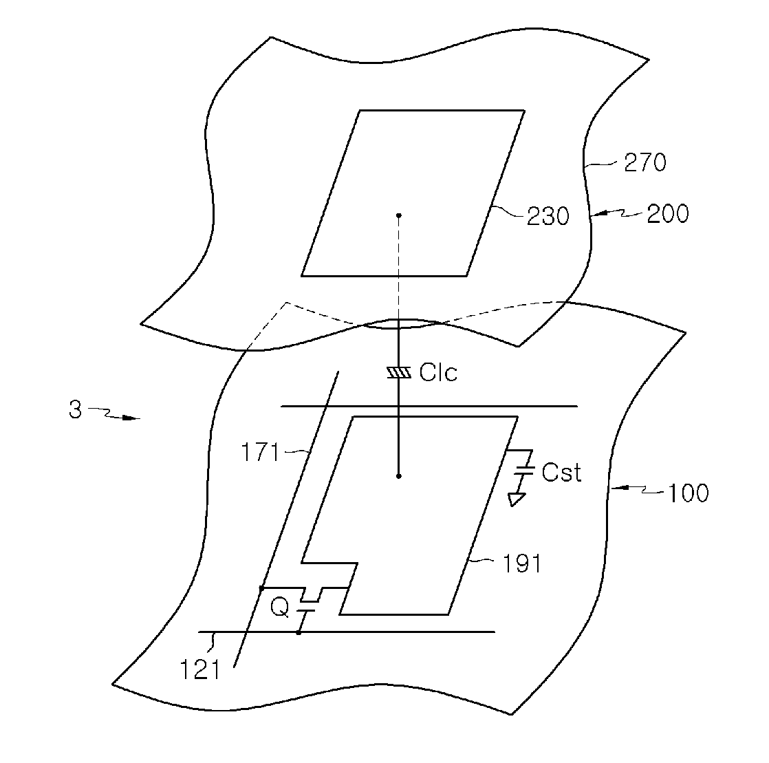
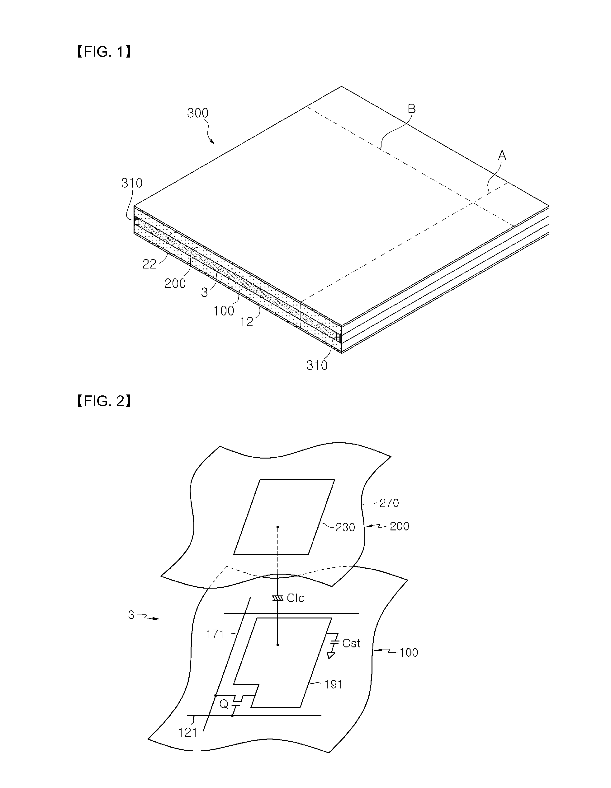
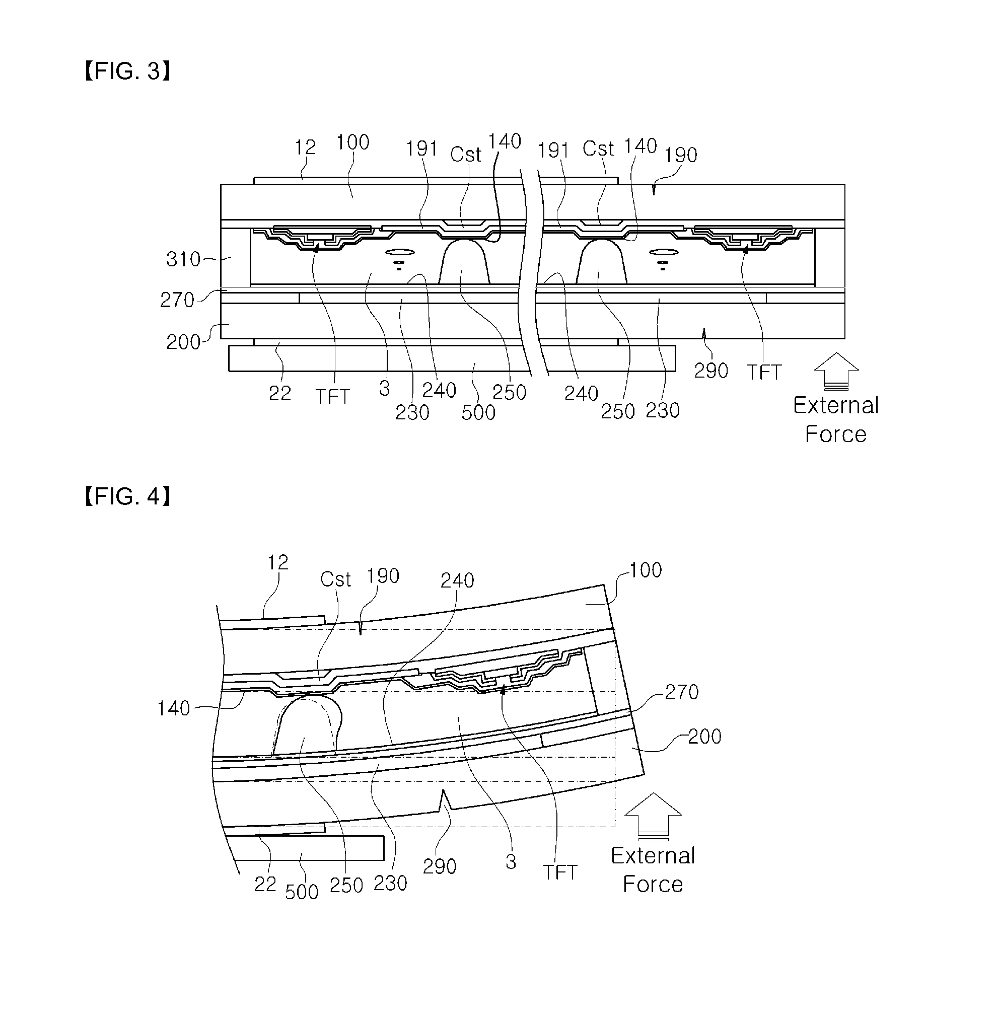
FIELD OF THE INVENTION[0001]The present invention relates to a method for manufacturing a multi-display device.BACKGROUND ART[0002]A liquid crystal display device is widely used due to various advantages such as light-weight, thin thickness, low electric power consumption.[0003]Generally, a liquid crystal display (LCD) includes two display panels and a liquid crystal layer disposed therebetween and having a dielectric anisotropy. An electric filed is formed in the liquid crystal layer, and a transmittance of light passing the liquid crystal layer is regulated by regulating amplitude of the electric field so as to obtain a desired image. Such a liquid crystal display is representative one of a flat panel display (FPD), and TFT-LCD which uses thin film transistor (TFT) as a switching element is widely used.[0004]A plurality of display signal lines i.e., gate lines and data lines, a plurality of thin film transistors and pixel electrodes are formed on a lower display panel of the two d...

Claims


Application Information

Patent Timeline
IPC IPC(8): B23P11/00
CPCG02F1/13336Y10T29/49826G02F1/133528G02F1/1333G02F1/1339G02F1/13
Inventor KIM, YONG BEOMKIM, DONG HYUN
Owner TOVIS
Learn More