
Method and apparatus for adjusting the gain of an amplifier of an optical receiver module based on link bit error rate (BER) measurements

an optical receiver and amplifier technology, applied in the field of optical communication systems, can solve the problems of reducing the bandwidth of the tia, limiting the design of the optical system, and limited link performance,

Inactive Publication Date: 2012-07-12
AVAGO TECH WIRELESS IP SINGAPORE PTE
View PDF2 Cites 23 Cited by
  • Summary
  • Abstract
  • Description
  • Claims
  • Application Information

AI Technical Summary

Benefits of technology

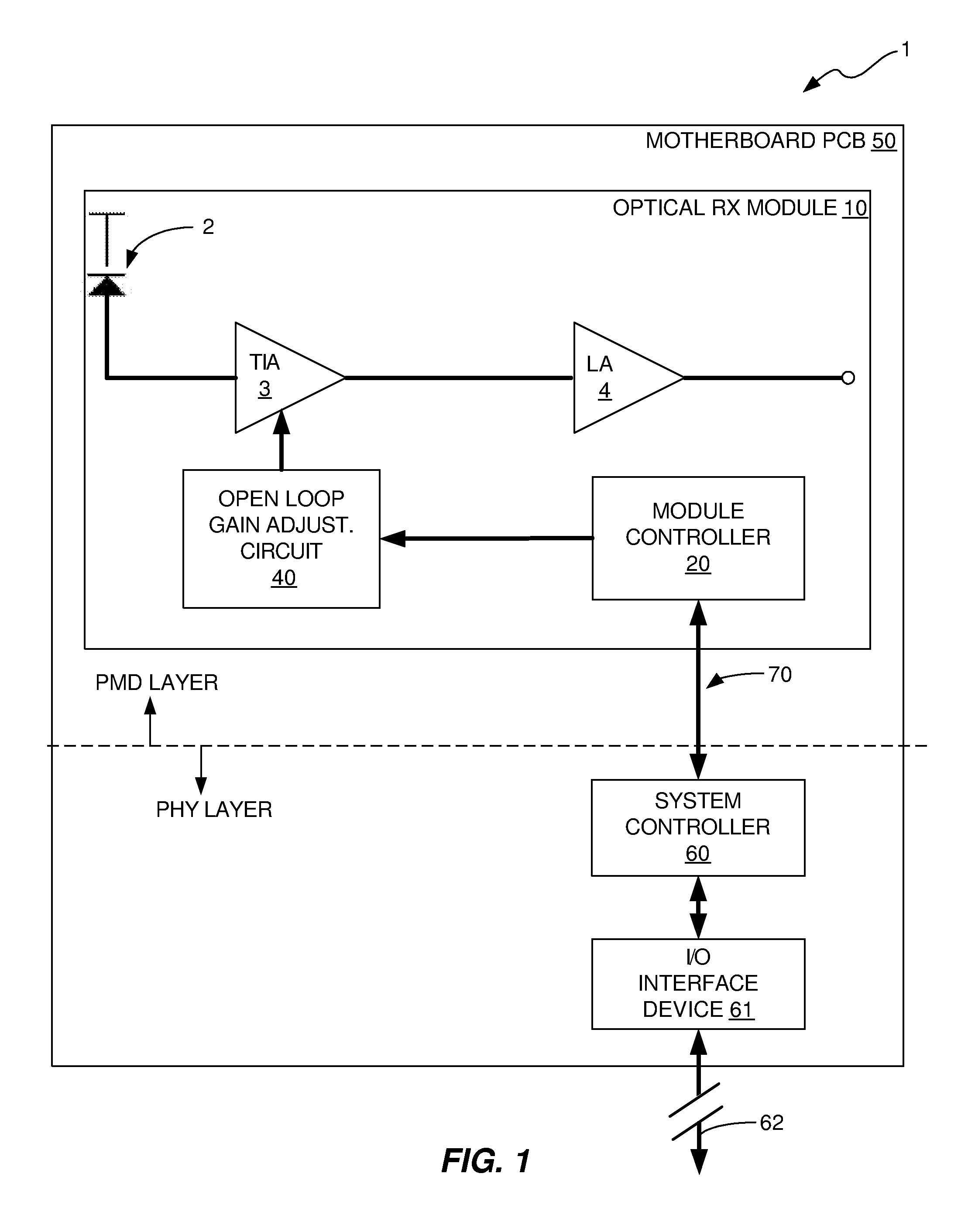
[0012]The invention is directed to an apparatus and method for adjusting the gain of a transimpedance amplifier (TIA) of an optical receiver (RX) module of an optical communications device based on link bit error rate (BER) measurements. The apparatus comprises an open loop gain adjustment circuit of the optical RX module and a module controller of the optical RX module. The gain adjustment circuit is configured to adjust the gain of the TIA of the optical RX module. The module controller of the optical RX mod

Problems solved by technology

The link performance is also limited by the maximum power that the receiver can tolerate before the receiver experiences a condition known as receiver overload.
The overall dynamic range available in the optical receiver often limits the design of an optical system.
In general, an increase in the gain of the TIA, for a given amount of power dissipation, results in a decrease in the bandwidth of the TIA.
Increasing the gain of the TIA reduces the input-referred noise, but reduces the bandwidth of the TIA.
Increasing the gain of the TIA, however, can result in voltage swings in the TIA that cause receiver overload.
Receiver overload is observed when bipolar devices are pushed into saturation or CMOS devices are pushed into linear operation.
When this happens, a large increase in jitter is observed, which is due to a decrease in the speed of the data transitions.
For transistors made using advanced process technologies, device breakdown voltage presents a limit that cannot be overcome.
However, these techniques are only successful over a limited range of input signal swing.
There are challenges and drawbacks associated with typical AGC circuit architectures.
One drawback is that it can be difficult for the closed feedback loop to achieve stability.
To support longer run lengths of bits, the bandwidth of the feedback loop must be made smaller, which can result in large amounts of silicon real estate being consumed by the AGC circuit.
Another drawback associated with typical AGC circuits is that the mechanism for adjusting the gain is usually a passive resistor in parallel with a metal oxide semiconductor (MOS) active resistor.
The MOS active resistor has more parasitic capacitance than the passive resistor, which reduces the upper bandwidth of the receiver and also contributes more noise.
Yet another drawback associated with typical AGC circuits is that they have higher power dissipation due to the feedback circuits and the larger bias currents needed to overcome the parasitic capacitance of the variable resistance.

Method used


Image

  • Method and apparatus for adjusting the gain of an amplifier of an optical receiver module based on link bit error rate (BER) measurements
  • Method and apparatus for adjusting the gain of an amplifier of an optical receiver module based on link bit error rate (BER) measurements
  • Method and apparatus for adjusting the gain of an amplifier of an optical receiver module based on link bit error rate (BER) measurements

Examples


Embodiment Construction

[0018]In accordance with the invention, an open loop gain adjustment method and apparatus are provided for adjusting the gain of a TIA of an optical RX module based on measurements of the BER of the optical link in which the optical RX module is employed. The gain of the TIA is adjusted until a determination is made that a satisfactory or optimum link BER has been achieved. The apparatus and method will now be described with reference to a few illustrative or exemplary embodiments.

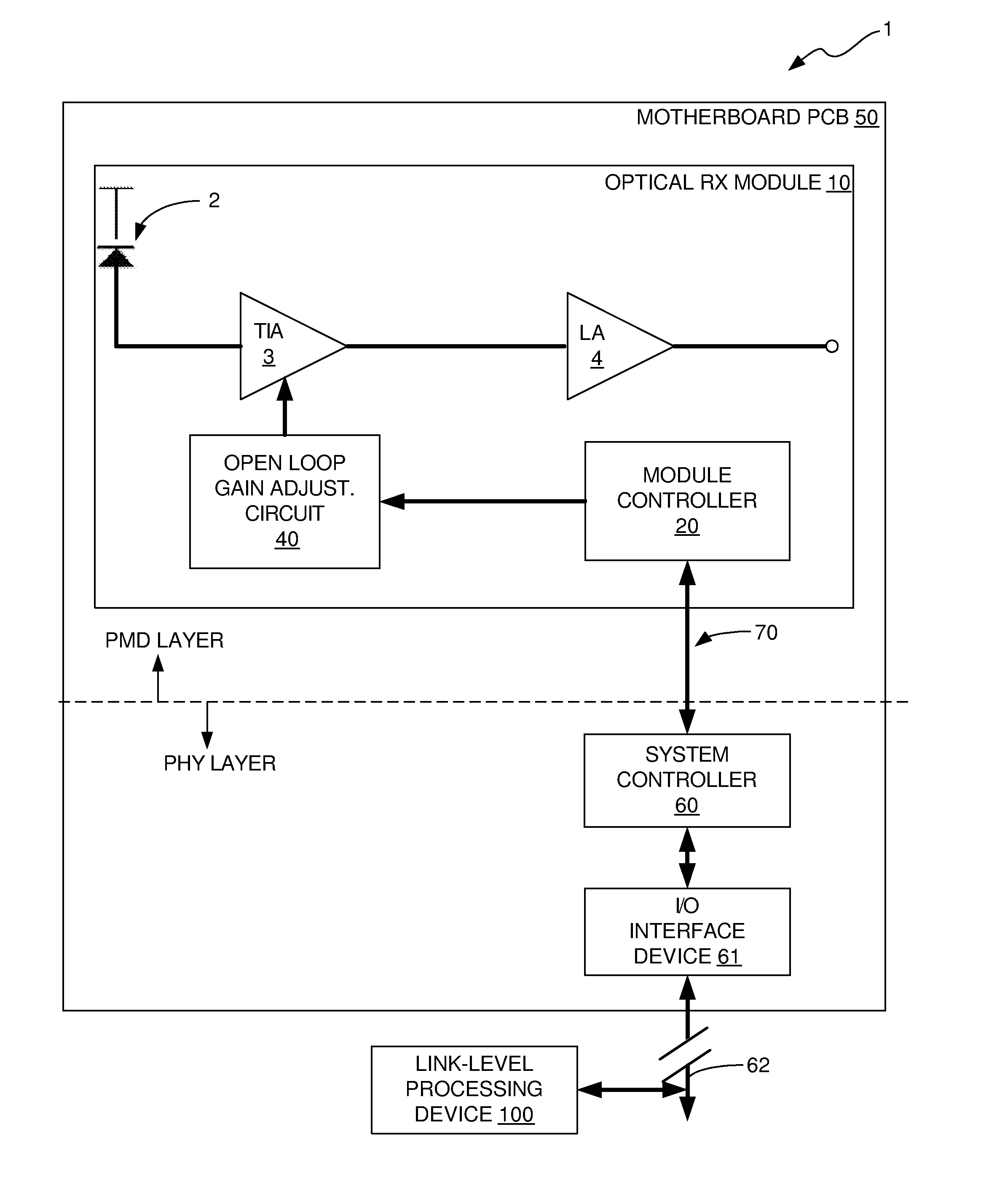
[0019]FIG. 1 illustrates a block diagram of an optical communications system 1 in which the gain of a TIA 3 of an optical RX module 10 is adjusted based on BER measurements obtained by a system level controller 60 that is external to the optical RX module 10. The optical RX module 10 is mounted on a motherboard printed circuit board (PCB) 50 of the optical communications system 1. The optical communications system 1 typically also includes a TX module (not shown), but for ease of illustration and for clari...


PUM


Abstract

An open loop gain adjustment method and apparatus are provided for adjusting the gain of a TIA of an optical RX module based on measurements of the BER of the optical link in which the optical RX module is employed. The gain of the TIA is adjusted until a determination is made that a satisfactory or optimum link BER has been achieved.

Description

TECHNICAL FIELD OF THE INVENTION[0001]The invention relates to optical communications systems. More particularly, the invention relates to a method and an apparatus for adjusting the gain of an amplifier of an optical receiver module based on link bit error rate (BER) measurements.BACKGROUND OF THE INVENTION[0002]A typical optical transceiver module currently used in optical communications includes a transmitter portion and a receiver portion. The transmitter (TX) portion includes a laser driver, which is typically an integrated circuit (IC), one or more laser diodes, and an optics system. The laser driver outputs electrical signals to the laser diodes to modulate them. When the laser diodes are modulated, they output optical signals, which are then directed by the optics system of the TX portion onto the ends of respective transmit optical fibers or waveguides held within a connector that mates with the transceiver module. The TX portion typically also includes an open loop or clos...

Claims


Application Information

Patent Timeline
IPC IPC(8): H04B10/08
CPCH04B10/6931H04B10/07953
Inventor MILLER, FREDERICK W.
Owner AVAGO TECH WIRELESS IP SINGAPORE PTE
Learn More