Silicon photomultiplier with trench isolation

Inactive Publication Date: 2012-06-21
ELECTRONICS & TELECOMM RES INST
View PDF5 Cites 25 Cited by
  • Summary
  • Abstract
  • Description
  • Claims
  • Application Information

AI Technical Summary

Benefits of technology

[0027]Embodiments of the present invention are directed to a silicon photomultiplier with trench isolation for maintaining the photon detection efficiency high while increasing the dynamic range of light intensity measurement, by reducing the degradation of the effective fill factor that follows the increase of cell number density intended for a dynamic range enhancement.
[0028]Embodiments of the present invention are also directed to a silicon photomultiplier with trench isolation for increasing the effective fill factor of a device by multifunctionalizing the trench structure.
[0029]Embodiments of the present invention are also directed to a silicon photomultiplier with trench isolation for additionally increasing the effective fill factor of a device and uniformizing the breakdown characteristics of the cell diodes, by improving the shape of cells and their arrangement in a device.
[0037]As mentioned above, according to the present invention, the photo detection efficiency can be maintained high and the light intensity measurement dynamic range can be increased by reducing the deterioration of the effective fill factor inevitably following the cell number densification through the trench isolation structure.
[0038]In addition, the effective fill factor of a device can be increased and the performance can be improved by minimizing distances between cells through blocking photons leaking among cells by ameliorating the trench isolation structure and multifunctionalizing the trench to function as quench resistor and guard ring at the same time.
[0039]Further, it is possible to additionally increase the effective fill factor of a device and uniformize the breakdown characteristics of the light-receiving areas by using hexagonal cells in honeycomb arrangement to improve the cell shape and arrangement structure over the general quadrilateral structure.

Problems solved by technology

When an electrical breakdown occurs in a cell, the cell cannot operate for a while and if a large current continuously flows through the cell after the breakdown, the device may be damaged.
If the high energy photons reach the adjacent cells, additional breakdowns can occur in the adjacent cells.
If the probability of such an additional breakdown were close to 1, the breakdown would successively spread to the adjacent cells, making the multicell design of the device pointless.
However, such a design is not adequate for silicon photomultipliers with small cell sizes.
Such reduction of the effective fill factor deteriorates the photon detection efficiency of the device.

Method used


Image

  • Silicon photomultiplier with trench isolation
  • Silicon photomultiplier with trench isolation
  • Silicon photomultiplier with trench isolation

Examples


Embodiment Construction

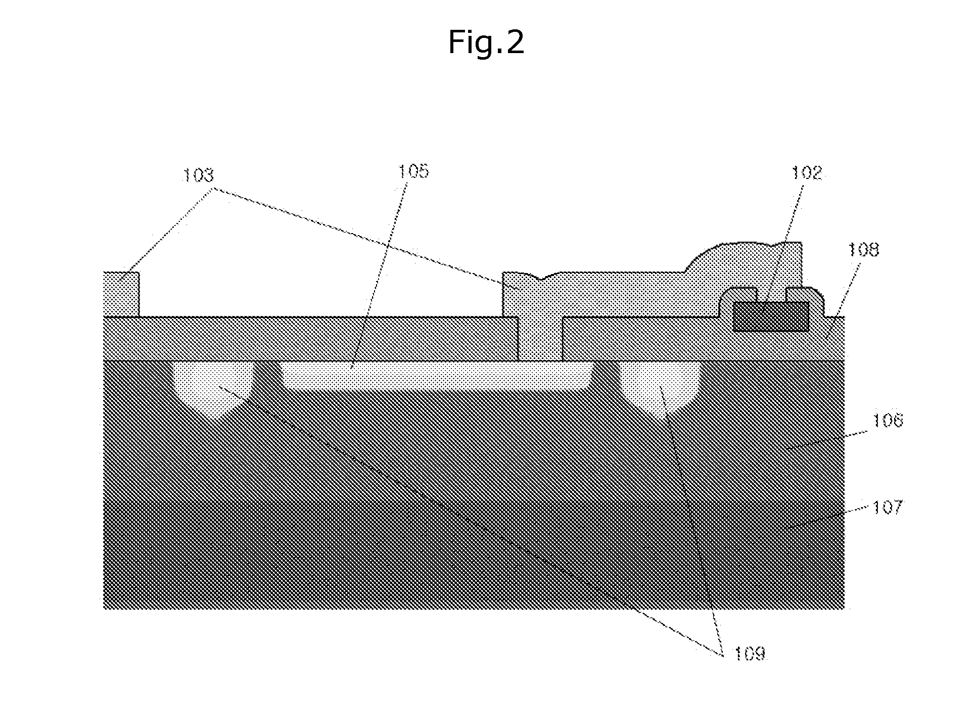
[0046]Hereinafter, a silicon photomultiplier with trench isolation in accordance with the present invention will be described in detail with reference to the accompanying drawings. In the drawings, the thicknesses of lines or the sizes of elements may be exaggeratedly illustrated for clarity and convenience of description. Moreover, the terms used henceforth have been defined in consideration of the functions of the present invention, and may be altered according to the intent of a user or operator, or conventional practice. Therefore, the terms should be defined on the basis of the entire content of this specification.

[0047]FIG. 3 illustrates a schematic plan view of a silicon photomultiplier according to an embodiment of the present invention, FIG. 4 illustrates a cross-sectional view of the device in FIG. 3, taken along the lines b-b′ and c-c′, and FIG. 5 illustrates a graph of the device fill factor comparing between hexagonal and square cell of the silicon photomultiplier.

[0048...


PUM


Abstract

The present invention relates to a silicon photomultiplier with trench isolation for maintaining the photon detection efficiency high while increasing the dynamic range, by reducing the degradation of the effective fill factor that follows the increase of cell number density intended for a dynamic range enhancement.

Description

CROSS-REFERENCE TO RELATED APPLICATIONS[0001]The present application claims priority to Korean patent application number 10-2010-0131869, filed on Dec. 21, 2010, which is incorporated by reference in its entirety.BACKGROUND OF THE INVENTION[0002]The present invention relates to a silicon photomultiplier having an improved performance through the structure improvement.[0003]Typical silicon photomultipliers basically have a planar diode structure and is generally composed of doped layers of p+-p-n+ or n+-n-p+. As the reverse voltage applied to such a diode structure is increased, the depletion layer between p+ and n+ is expanded, and when the voltage becomes higher than the breakdown voltage, an electrical breakdown occurs.[0004]The avalanche mode is an operation mode using the phenomenon that, when the above device operates as a photo-sensor with an applied voltage a little bit lower than the breakdown voltage, input photons are changed into pairs of charge carriers inside the semico...

Claims


Application Information

Patent Timeline
IPC IPC(8): H01L27/142
CPCH01L27/1446H01L31/103H01L27/1463H01L27/14H01L31/101
Inventor LEE, JOON SUNG
Owner ELECTRONICS & TELECOMM RES INST
Why Eureka
Try Eureka