Grating coupler and package structure incorporating the same
a technology of grating couplers and package structures, applied in the direction of optics, instruments, optical light guides, etc., can solve the problems of high cost, inconvenient mass production, and incompatible grating coupler fabrication technology with conventional cmos
- Summary
- Abstract
- Description
- Claims
- Application Information
AI Technical Summary
Benefits of technology
Problems solved by technology
Method used
Image
Examples
Embodiment Construction
[0013]The disclosure is illustrated by way of example and not by way of limitation in the figures of the accompanying drawings in which like references indicate similar elements. It should be noted that references to “an” or “one” embodiment in this disclosure are not necessarily to the same embodiment, and such references mean at least one.
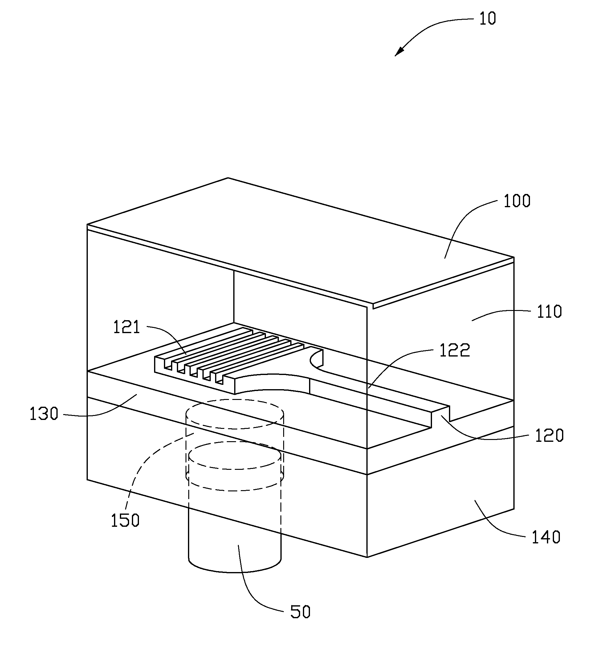
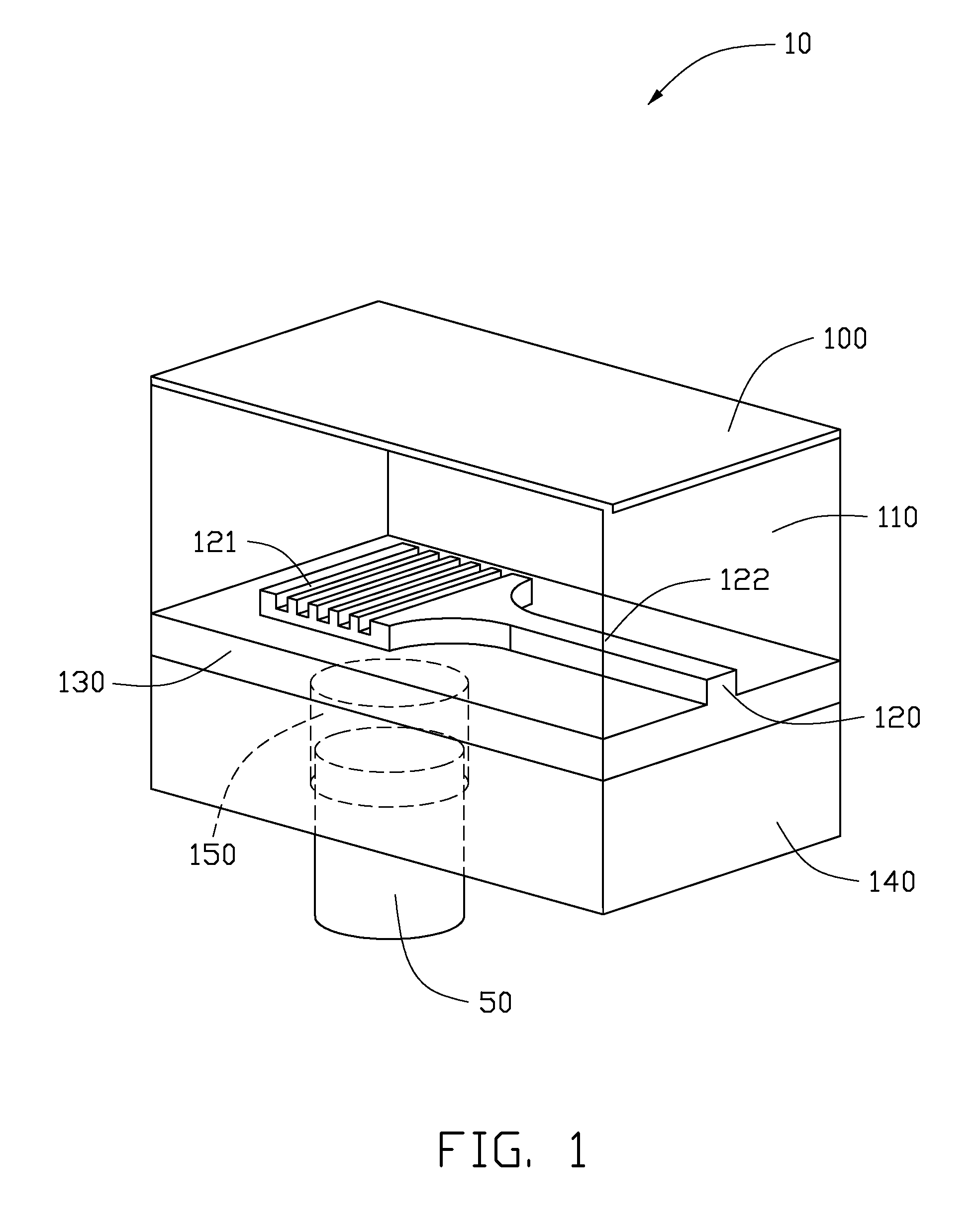
[0014]Referring to FIG. 1 and FIG. 2, one embodiment of a grating coupler 10 includes a reflector layer 100, an isolation layer 110, a waveguide layer 120, an under-cladding layer 130, and a substrate 140. The substrate 140 has a first surface 141, an opposite second surface 142, and a third surface 143 extending between the first surface 141 and the second surface 142. The under-cladding layer 130 is disposed on the first surface 141. The reflector layer 100, the isolation layer 110, the waveguide layer 120, and the under-cladding layer 130 are stacked on each other in sequence along a direction from the first surface 141 to the second surface 1...
PUM
 Abstract
Description
Claims
Application Information
 - R&D
- Intellectual Property
- Life Sciences
- Materials
- Tech Scout
- Unparalleled Data Quality
- Higher Quality Content
- 60% Fewer Hallucinations
Browse by: Latest US Patents, China's latest patents, Technical Efficacy Thesaurus, Application Domain, Technology Topic, Popular Technical Reports.
© 2025 PatSnap. All rights reserved.Legal|Privacy policy|Modern Slavery Act Transparency Statement|Sitemap|About US| Contact US: help@patsnap.com


